

Application of Hole-Transporting Materials as the Interlayer in Graphene Oxide/Single-Wall Carbon Nanotube Silicon Heterojunction Solar Cells*
LePing Yu A , Tom Grace A , Hong Duc Pham B , Munkhbayar Batmunkh A , Mahnaz Dadkhah A , Cameron Shearer A , Prashant Sonar B and Joe Shapter A CA Centre for Nanoscale Science and Technology, School of Chemical and Physical Sciences, Flinders University, Bedford Park, SA 5042, Australia.
B School of Chemistry, Physics and Mechanical Engineering, Queensland University of Technology (QUT), Brisbane, Qld 4001, Australia.
C Corresponding author. Email: joe.shapter@flinders.edu.au
Australian Journal of Chemistry 70(11) 1202-1211 https://doi.org/10.1071/CH17380
Submitted: 6 July 2017 Accepted: 9 August 2017 Published: 31 August 2017
Abstract
Solid-state hole-transporting materials, including the traditional poly(3,4-ethylenedioxythiophene):poly(styrene sulfonate) (PEDOT:PSS), and recently developed 4,4′-(naphthalene-2,6-diyl)bis(N,N-bis(4-methoxyphenyl)aniline) (NAP) and (E)-4′,4‴-(ethene-1,2-diyl)bis(N,N-bis(4-methoxyphenyl)-[1″,1‴-biphenyl]-4-amine) (BPV), have been applied as a hole-transporting interlayer (HTL) for graphene oxide/single-walled carbon nanotube–silicon (GOCNT/Si) heterojunction solar cells, forming a GOCNT/HTL/Si architecture. The influence of the thickness of the HTL has been studied. A new AuCl3 doping process based on bath immersion has been developed and proved to improve the efficiency. With the AuCl3-doped GOCNT electrodes, the efficiency of GOCNT/PEDOT:PSS/Si, GOCNT/NAP/Si, and GOCNT/BPV/Si devices was improved to 12.05 ± 0.21, 10.57 ± 0.37, and 10.68 ± 0.27 % respectively. This study reveals that the addition of an HTL is able to dramatically minimise recombination at the heterojunction interface.
Introduction
Over the past several decades, carbon-based materials, including carbon nanotubes (CNTs)[1–6] and graphene,[7–10] have been widely studied and applied in photovoltaics owing to their outstanding optoelectronic properties. Graphene oxide (GO), a derivative of the 2-D material graphene containing hydrophilic functional groups, such as hydroxyl, carboxyl and epoxy groups on the edges or over the basal plane, has been used as an amphiphilic material in the preparation of CNT aqueous dispersions.[11–13] In the fabrication of a transparent conducting film, the porous and disconnected regions of CNT networks can be filled in with GO sheets, which offer additional transport paths in a composite film (GOCNT).[14] More importantly, compared with pure CNT films, GOCNT composite films with both hydrophobic and hydrophilic groups offer much better compatibility in both organic solvents and water, with dramatically enhanced mechanical properties providing great advantages in solution-based processing.[15,16]
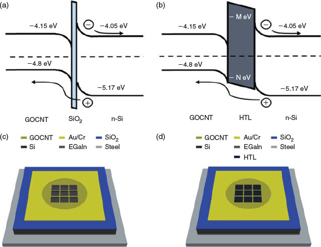
Photovoltaics based on the heterojunction created between silicon (Si) and GOCNT hybrid film, GOCNT/Si, have been studied extensively.[14] In such a device, as shown in Fig. 1a, light absorption in Si creates excitons that then diffuse and are separated into free charge carriers with the help of the built-in potential at the interface of the heterojunction. If the device is considered a p-typed GOCNT/n-type silicon heterojunction, the separated holes and electrons are collected at the GOCNT films and Si respectively.[17–19] However, there is still considerable discussion about the exact nature of the heterojunction with researchers labelling it a Schottky junction, metal–insulator–semiconductor, or p-n junctions.[20] In most cases, there is a thin layer of SiO2 between the Si and top hybrid film, which reduces the reverse saturation current and increases the lifetime of the minority carriers, and therefore enhances the diode properties.[21]
|
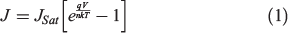
A few studies have shown that the addition of an extra interlayer of conducting polymers, such as polyaniline,[22] poly(3-hexylthiophene-2,5-diyl) (P3HT),[23] and poly(3,4-ethylenedioxythiophene):poly(styrene sulfonate) (PEDOT:PSS), between Si and CNT can improve the performance of the CNT/Si devices.[23] Recently, 2,2′,7,7′-tetrakis(N,N′-di-p-methoxyphenylamine)-9,9′-spirobiuorene (spiro-OMeTAD), which plays the same role in a GOCNT/Si solar cell, has successfully improved efficiency to above 13 %[24] owing to improved hole transport.[25–27] In addition to these traditional materials, there are also some recently synthesised new low-cost hole-transporting layer (HTL) materials, which have been successfully applied in perovskite solar cells, such as 4,4′-(naphthalene-2,6-diyl)bis(N,N-bis(4-methoxyphenyl)aniline) (NAP)[28] and (E)-4′,4‴-(ethene-1,2-diyl)bis(N,N-bis(4-methoxyphenyl)-[1″,1‴-biphenyl]-4-amine) (BPV) with comparable efficiency to that of spiro-OMeTAD.[29] Based on these ideas, these new materials, as well as PEDOT:PSS, which have been widely used in many other devices, including dye-sensitised solar cells,[30–33] perovskite solar cells,[34–36] and organic photovoltaics,[37–39] may be able to improve the performance of GOCNT/Si solar cells by serving as an HTL and thus enhance diode properties with limited light absorption at the same time, as shown in Fig. 1b.
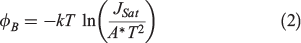
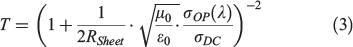
In the present report, we apply three different hole-transporting materials (PEDOT:PSS, NAP, and BPV) as the HTL between Si and the transparent conducting GOCNT hybrid film (GOCNT/PEDOT:PSS/Si, GOCNT/NAP/Si, and GOCNT/BPV/Si). In order to see the influence of the addition of HTL, control devices built with GOCNT and Si were prepared, as pictured in Fig. 1c, d. Optimisation of the thickness of HTL was conducted to maximise the efficiency of the devices. The effect of doping on GOCNT using a gold chloride (AuCl3) bath was studied as well.
Results and Discussion
Characterisation of the Starting Materials and Transparent Conducting Electrodes
In order to estimate the quality of the GO, three different techniques were used to analyse the GO stock solution, as shown in Fig. S1 (Supplementary Material). First, the diluted GO stock solution (0.017 mg mL−1) shows a broad absorption band with a peak at 227 nm (assigned to π–π* transitions), a shoulder at ~300 nm (assigned to n–π* transitions of C=O), and a long tail over the visible range to 800 nm or even further, as shown in Fig. S1a (Supplementary Material), which is consistent with the literature.[40,41] Second, Raman spectroscopic measurements show that the pure GO film prepared from the GO stock solution has two main features, as shown in Fig. S1b (Supplementary Material), the D band at 1332 cm−1 (breathing mode of A1g symmetry) and the G band at 1587 cm−1 (E2g symmetry of sp2 carbon atoms), which are in agreement with the literature values.[42] The D band signal is related to the defects on the graphene structure and caused by out-of-plane vibrations whereas the G band signal is a result of in-plane vibrations of sp2-bonded carbon atoms. Generally, the oxygen-rich groups introduced by functionalisation on the graphene plane contribute to the D band intensity and a lower G/D ratio infers higher defect content.[43] Here, the G/D ratio is 0.93, indicating that there are many functional groups. In addition, scanning electron microscope (SEM) images (Fig. S1c, Supplementary Material) show that most of GO sheets seem to be well dispersed in the stock solution but there still exist some aggregates in the stock solution (Fig. S1c, inset) and mild sonication for 20 min is possibly not enough to separate all flakes into individual sheets. Compared with the literature value (2 min),[44] the sonication period is 10 times longer, which is partially due to the lower power output for the sonicator used in the present experiment compared with the one used in the literature (80 versus 100 W). Overall, GO was successfully synthesised and a high-quality aqueous dispersion was formed.
Four different characterisation techniques were used to evaluate the properties of the GOCNT hybrid films before and after AuCl3 doping, as shown in Fig. 2. The UV-vis-near infrared (NIR) spectra show that the as-prepared film has a broad absorbance feature above 1500 nm with a reasonably sharp peak at ~1100 nm (Fig. 2a), which were assigned to absorbance from the first and second van Hove singularities of the semiconducting arc-discharged single-wall carbon nanotubes (SWCNTs) (S11 and S22).[45] The transmittance (T) of the film is 85 %, which is characterised by the absorbance (A) at 550 nm. The Raman spectrum (Fig. 2b) shows a G band with a clear metallic contribution in the low-energy area in the as-prepared film because of the strong electron–phonon interactions.[46,47] Sheet resistance (Rsheet) of the as-prepared film is 1404 ± 8.4 Ω sq−1 with a calculated figure of merit (FOM) of 1.58 ± 0.01, as shown in Fig. 2c, and these values are similar to those of the GOCNT films in our previous studies.[24] A SWCNT network covered with and interspersed with GO sheets is observed in the SEM image of the as-prepared film (Fig. 2d), and can be contrasted with the wrinkle features in pure GO and the network structure in pure CNT film (Fig. S2a, b, Supplementary Material). After doping the as-prepared film in an AuCl3 acetone bath, the S11 peak disappears completely while the intensity of the S22 peak is partly suppressed and the T at 550 nm of the film decreases slightly from 85 to 84 % (Fig. 2a). In terms of the Raman signal (Fig. 2b), there is a reduction in the contribution of G band from the metallic species, with an upshift in peak position from 1585 to 1598 cm−1, which suggests charge extraction from SWCNTs to the dopant (AuCl3) and resulting phonon stiffening.[48,49] As a result of doping, the optoelectronic properties of the GOCNT hybrid films are improved, as shown in Fig. 2c, with decreased Rsheet (882 ± 2.1 Ω sq−1) and increased FOM (2.34 ± 0.01) (a higher FOM value indicates better optoelectronic properties[50]). In addition, gold nanoparticles (AuNPs, the bright spots in Fig. S2c, Supplementary Material) are observed through the entire film in the SEM image (Fig. 2d). The number of nanoparticles (NPs) per unit area on the GOCNT surface was used to characterise the distribution of the NPs, as shown in the SEM image (Fig. 2d). There are 168 Au NPs over the GOCNT surface with an area of ~90 µm2, and thus the number of NPs per unit area is 1.86 particles µm−2. In addition, the size of these NPs is between 100 and 250 nm in diameter. The exact doping mechanism is still under discussion. Most researchers assign the p-type doping to the reduction of Au3+ to Au, but others think that the formation of SWCNT-Cl plays an important role with the electrons of SWCNTs withdrawn to Cl.[51]

|
Initial Testing of Photovoltaic Devices
The performance of three sets of devices, GOCNT/Si, HTL/Si, and GOCNT/HTL/Si, is shown in Fig. 3, Table 1, and Fig. S3 (Supplementary Material). The devices without GOCNT hybrids films, HTL/Si (including PEDOT:PSS/Si, NAP /Si, and BPV/Si) have the poorest performance among these three sets, with the lowest open circuit voltage (VOC (below 0.5 V), Fig. 3a), fill factor (FF (less than 0.2), Fig. 3a), and limited generation of photocurrent (or short-circuit current density (JSC) less than 2 mA cm2) from 300 to 1100 nm (Fig. 3b). The poor efficiency of these devices may be due to significant recombination of the separated holes and electrons (indicated by the terrible diode properties (highest ideality (above 2.5) and reverse saturation current (Jsat ~10−4 mA cm−2, calculated by Eqn 1) as shown in Fig. 3c and lowest Schottky barrier height ΦB (~0.8 eV) related to the extremely high Rsheet of the HTL (in the order of 106 Ω sq−1) as well as long charge transport distance to the metal grid lines.

|

|
The role of the GOCNT was studied with the addition of hybrid films on HTL-coated Si (GOCNT/HTL/Si). As shown in Table 1, the efficiency was significantly improved to 9.74 ± 0.31, 6.85 ± 0.36, and 8.68 ± 0.25 % for GOCNT/PEDOT:PSS/Si, GOCNT/NAP/Si, and GOCNT/BPV/Si, with increased JSC to above 27 mA cm−2, VOC to above 0.52 V, and FF to above 0.45. Noticeably, the efficiency of GOCNT/PEDOT:PSS/Si approaches the best CNT/Si devices before any chemical doping (12.4 %).[52] This improvement can be attributed to the dramatic enhancement in diode properties, with ideality decreasing to less than 1.3, Jsat minimised to less than 4 × 10⁻⁶ mA cm−2 and ΦB improved to above 0.89 eV, which indicates that the addition of GOCNT hybrid films reduces the recombination of the separated carriers by collecting and transporting them to the electrode because of the much lower Rsheet (below 2000 Ω sq−1).
The role of the HTL was further studied by comparing the performance of GOCNT/Si and GOCNT/HTL/Si devices, as shown in Fig. 3, Table 1 and Fig. S3 (Supplementary Material). The efficiency of GOCNT/Si (4.63 ± 0.53 %) is lower than any type of GOCNT/HTL/Si devices. Specifically, the JSC for both GOCNT/Si and GOCNT/HTL/Si devices is similar. The HTL-based devices seem to generate more photocurrent in the high-wavelength range (Fig. 3d–f), but actually this is due to the absorbance of light by HTL materials below 550 nm, which is similar to what was observed in our previous study.[24] The improvement of the performance is mainly due to the increased VOC. With the HTL, the devices have better diode properties with lower ideality and Jsat and higher ΦB, which is used to estimate recombination, with lower values corresponding to more serious recombination, lower FF and VOC. As discussed earlier, the heterojunction formed by GOCNT and Si is not an ideal Schottky junction and hence ΦB is calculated from Eqn 2, which assumes a simpler model. Furthermore, it was shown that the addition of a conducting polymer interlayer in graphene/Si devices leads to an increased ΦB.[53] Compared with GOCNT/HTL/Si devices, the lower VOC, FF, ΦB, and worse diode properties of GOCNT/Si indicate that the HTL may effectively benefit the separated hole being transported from Si to GOCNT and block the separated electron at the same time.
Thickness of HTLs
In order to study the influence of the HTL thickness on solar cell performance, the same amount of stock solution was applied on the Si substrates with different spin speeds (1000, 3000, 5000, and 7000 rpm). As shown in Figs S4–S6 (Supplementary Material), the thicknesses of the PEDOT:PSS layers (applied from 1000 to 7000 rpm) are 40, 30, 20, and 10 nm; for NAP, they are 90, 70, 50, 30 nm (applied from 1000 to 7000 rpm); and for BPV, they are 85, 65, 50, 30 nm (applied from 1000 to 7000 rpm). It is worth noting that PEDOT:PSS forms pinhole-free films whereas there are some pinholes in the other two films (see atomic force microscopy (AFM) data in the Supplementary Material). Solar cells with different HTL thicknesses between the GOCNT and Si substrate were prepared and tested, with the details illustrated in Fig. 4 and Fig. S7 (Supplementary Material).

|
The current density versus voltage (J–V) light curves are shown in Fig. S7a–c (Supplementary Material). In the GOCNT/PEDOT:PSS/Si and GOCNT/NAP/Si architecture, the efficiency peaks for devices coated with 20- and 70-nm HTL (11.00 ± 0.17 and 9.71 ± 0.19 %, Fig. 4a) respectively whereas it is difficult to assign the best thickness value of BPV for GOCNT/BPV/Si devices owing to the quite large error bars but the optimal thickness may be between 50 and 65 nm. For all three types of devices, there seems to be a clear dependence between the efficiency and both the FF and VOC, as shown in Fig. 4b, c. Both FF and VOC increase with thickness of the HTLs at first, then decrease when the HTL is thicker, especially for GOCNT/PEDOT:PSS/Si and GOCNT/NAP/Si devices. This trend is because a better heterojunction is formed initially, with the increase in thickness providing decreased recombination at first, but when the film is very thick, the ability to transport holes collected from Si to the GOCNT electrode decreases.[24] In terms of the photocurrent, the general trend is that it decreases with increase in HTL thickness, as shown in Fig. 4d. This decreasing trend can be explained by the external quantum efficiency (EQE) measurements (Fig. S7d–f, Supplementary Material) where the absorbance of HTL material in the low-wavelength range increases with thickness and thus fewer excitons are created in the Si with less photocurrent produced. In addition to the efficiency-relevant parameters (FF and VOC), the efficiency of the devices also seems to be dependent on both Rshunt (in a similar trend, Fig. 4e) and Rseries (in a reverse trend, Fig. 4f). The diode properties are summarised in Fig. 4g–i with the J–V dark curves illustrated in Fig. S7g–i (Supplementary Material). Owing to the quite large error bars, it is difficult to draw any conclusions from these devices although it still seems that the devices with the optimised HTL thickness have better diode properties (lower ideality and Jsat but higher ΦB) than those with very thick HTL. Therefore, when the thickness of PEDOT:PSS is 20 nm (and for NAP and BPV, 70 nm and somewhere between 50 and 65 nm), the HTL is thick enough to create an ideal heterojunction as well as thin enough to transport holes effectively from Si to GOCNT. The resulting devices have the highest efficiency.
AuCl3 Bath Doping
In order to further improve the performance of the devices, many dopants are available to reduce the Rsheet of GOCNT films.[54] For instance, AuCl3 aqueous solution was applied to the device surface by spin-coating in our previous study.[24] Here, a new doping process in an acetone bath is developed (refer to Experimental details), which can be potentially applied to transfer any floating GOCNT or thick CNT films onto any substrates without damaging the surface. The detailed effects of the AuCl3 doping on the performance of the solar cells (GOCNT/Si and GOCNT/HTL/Si with optimised HTL thickness) are summarised and plotted in Fig. 5 and Fig. S8 (Supplementary Material).

|
As shown in Fig. 5a, AuCl3 doping can improve the efficiency for all the devices, in which the performance of GOCNT/Si devices has the best improvement whereas the devices involving HTL show much less improvement. Generally, the devices have a slight decrease in JSC (Fig. 5b) due to the absorbance of the dopant, which is reflected in the reduction in the photocurrent in the low-wavelength range in EQE measurements (Fig. S8b, Supplementary Material). The VOC of all the GOCNT/HTL/Si devices are not influenced dramatically with doping although there is a clear increase for GOCNT/Si devices (Fig. 5c and Fig. S8a, Supplementary Material). The stable VOC of GOCNT/HTL/Si may be explained by the fact that the doping only changes the properties of the electrode and maintains the interface properties between Si and HTL where the separation of the excitons occurs (this corresponds to limited changes in the diode properties for the GOCNT/HTL/Si device, as shown in Fig. 5g–i and Fig. S8c, Supplementary Material). Similarly, one might simply attribute the improved VOC in GOCNT/Si devices to the change of the properties across the interface between GOCNT and Si. However, there is more behind this because it did not occur in our previous report where a reduced VOC was observed and was assigned to the possible short circuits caused by the AuNPs bridging the Si with the front metal electrode.[24,55] As the doping is performed in a different manner here, the possibility of bridging by AuNPs is probably reduced dramatically owing to the elimination of the contact between the AuCl3 stock solution and the Si surface during the doping. As the short circuits normally cause a change in the heterojunction diode properties and there is no significant change in ideality, Jsat, and ΦB for GOCNT/Si devices with AuCl3-doped electrodes (there even seems to be a slight improvement in these parameters; Fig. 5g–i and Fig. S8c, Supplementary Material), this is another piece of evidence showing that the presence of short circuits is greatly suppressed with the improved doping process. The most significant change in the properties of the GOCNT films by doping is the increase in conductivity and as a result, compared with as-prepared devices, FF and Rshunt are improved whereas a reduction in Rseries is observed with AuCl3-doped electrodes for all of the devices (GOCNT/Si and GOCNT/HTL/Si), as shown in Fig. 5d–f.
Conclusion
PEDOT:PSS, NAP, and BPV HTLs have been added between a GOCNT hybrid electrode and Si substrate to build GOCNT/HTL/Si solar cells. After optimisation of the HTL thickness, the efficiencies of GOCNT/PEDOT:PSS/Si, GOCNT/NAP/Si, and GOCNT/BPV/Si are 11.00 ± 0.17, 9.71 ± 0.19, and 9.78 ± 0.31 %. These numbers are further improved to 12.05 ± 0.21, 10.57 ± 0.37, and 10.68 ± 0.27 % with AuCl3-doped GOCNT top electrodes based on a bath immersion process. The major role of the interlayer is to transport holes while blocking electron transport from Si to GOCNT films after the separation of the excitons, therefore improving the heterojunction properties through a reduction in charge recombination.
Experimental Details
Synthesis of New Hole-Transporting Materials
Triphenyleamine (TPA) end capped TPA-NAP-TPA (NAP used here) and TPA-BPV-TPA (BPV used here) were synthesised and characterised according to previous reports and the synthesis details are given in the following.[28,29]
Synthesis of 4,4′-(Naphthalene-2,6-diyl)bis(N,N-bis(4-methoxyphenyl)aniline) (TPA-NAP-TPA)
In a round-bottom flask 2,6-bis(4,4,5,5-tetramethyl-1,3,2-dioxaborolan-2-yl)naphthalene (150 mg, 0.395 mmol), 4-bromo-N,N-bis(4-methoxyphenyl)aniline (455 mg, 1.184 mmol), and 2 M aqueous K2CO3 solution (12 mL) were dissolved in degassed toluene (18 mL). The solution was purged with argon for 15 min, then tetrakis(triphenylphosphine)palladium (16.18 mg 0.014 mmol) was added. The reaction was stirred at 120°C for 2 days. Then, the reaction mixture was cooled to room temperature and extracted with chloroform and water. The organic layer was dried over anhydrous Na2SO4 and concentrated by evaporation. After removing the solvent under reduced pressure, the residue was purified using silica gel column chromatography (eluent: hexane/ethyl acetate 10 : 1 v : v). Then, the crude product was recrystallised from hot methanol to yield the desired compound as a light brown solid (150 mg, 50 %). δH (600 MHz, CDCl3) 7.89 (s, 2H), 7.81–7.80 (d, J 8.4, 2H), 7.65–7.63 (dd, J1 8.4, J2 1.2, 2H), 7.48–7.47 (d, J 8.4, 4H), 7.03–6.96 (m, 12H), 6.79–6.77 (d, J 9.0, 8H), 3.73 (s, 12 H). δC (120 MHz, CDCl3) 155.93, 148.21, 140.88, 137.84, 132.92, 132.63, 128.45, 127.71, 126.65, 125.58, 124.39, 120.86, 114.74, 55.53. m/z (electrospray ionisation mass spectrometry (ESI-MS)) C50H42N2O4+• 734.50; calc. 734.31.
Synthesis of (E)-4′,4‴-(Ethene-1,2-diyl)bis(N,N-bis(4-methoxyphenyl)-[1″,1‴-biphenyl]-4-amine) (TPA-BPV-TPA)
In a round-bottom flask, (E)-1,2-bis(4-bromophenyl)ethene (150 mg, 0.443 mmol), 4-methoxy-N-(4-methoxyphenyl)-N-(4-(4,4,5,5-tetramethyl-1,3,2-dioxaborolan-2-yl)phenyl)aniline (439 mg, 1.02 mmol), and 2 M aqueous K2CO3 solution (12 mL) were dissolved in anhydrous toluene (18 mL). The solution was degassed with argon for 20 min, then tetrakis(triphenylphosphine)palladium (16 mg, 0.014 mmol) was added. Subsequently, the mixture was degassed for 30 min before the reaction was stirred at 120°C for 2 days. After the reaction mixture was cooled to room temperature and extracted with chloroform and water, the organic layer was dried over anhydrous Na2SO4 and then concentrated by evaporation. Purification of the crude product was carried out by using silica gel chromatography using a mixture of hexane and dichloromethane as eluent and then recrystallisation from hot acetone yielded the desired compound as a yellow solid (200 mg, 80 %). δH (600 MHz, CDCl3) 7.45 (d, J 8.8, 4H), 7.15 (s, 2H), 7.11 (d, J 8.8, 8H), 7.00 (d, J 8.4, 4H), 6.86 (d, J 8.8, 8H), 3.81 (s, 12H). δC (120 MHz, CDCl3) 155.87, 148.16, 140.80, 139.86, 135.65, 132.38, 127.85, 127.24, 126.86, 126.62, 120.64, 114.69, 55.53, 55.45. m/z (ESI-MS) C54H46N2O4+• 786.58; calc. 786.35.
Stock Solutions
The PEDOT:PSS aqueous dispersion (15 mg mL−1) was used as received (Clevios PVPAI 4083). Two solutions were prepared by dissolving 20 mg solid NAP or BPV in 1,2-dichlorobenzene with a final concentration of 5 mg mL−1. HAuCl4·3H2O (30 mL, 5 mM) (Sigma–Aldrich) solution for doping was prepared by dissolving 59 mg of the solid in acetone at room temperature with mild vortex mixing.
GO was prepared following the improved Hummers’ synthesis method developed by Marcano et al. with slight modifications.[56] Specifically, a mixture of 360 mL H2SO4 (98 %) and 40 mL H3PO4 (9 : 1) was added to a mixture of graphite flakes and KMnO4 (3 and 18 g). The reaction was heated at 50°C with stirring for 12 h. It was then cooled to room temperature and centrifuged at 1800 g for 4 h. The supernatant was discarded and the top 2/3 of the solid was collected and washed with water (200 mL), 30 % HCl (200 mL), and ethanol (200 mL twice) in succession. For each wash, the mixture was centrifuged at 1800 g for 4 h and the supernatant was disposed of while the top 2/3 of the solid content was collected for next wash. After the last wash, the solid was dried in a freeze-dryer overnight and the as-prepared GO collected. The as-prepared GO solids were suspended in deionised water with sonication for 20 min with a final concentration of 1 mg mL−1.
CNT (5 mg, P3-SWNT, Carbon Solutions Inc., USA) was suspended in 50 mL of deionised water by sonication for 1 h. GO stock dispersion (2 mL) was added with 45 mL CNT stock solution in order to target the ideal mass ratio of GO : CNT of 1 : 2.25 (according to our previous study, GOCNT hybrids with this ratio have ideal optoelectronic properties for application in solar cells).[14] The hybrid solution was further sonicated for 1.5 h, followed by centrifugation at 17500g for 1 h at 10°C to remove large agglomerates. The supernatant was collected and centrifuged one more time in the same manner. The second supernatant was collected and stored as the starting dispersion for the preparation of GOCNT hybrid film electrodes. All the sonication steps in the procedure were performed in an ice bath.
Fabrication of Hybrid Films
GOCNT hybrid films were prepared via vacuum filtration, which is similar to the procedure reported previously.[24] Specifically, 200 µL of GOCNT starting dispersion was diluted with deionised water to 100 mL. A mixed cellulose ester membrane (MCE, 0.45 µm, HAWP, Millipore) was used to collect GO and CNT. Beneath the MCE membrane was a nitrocellulose membrane (25 nm, VSWP, Millipore) with four holes (0.49 cm2 each) so that a faster flow rate at the areas of the four holes resulting from the different pore sizes of these two membranes produced four identical GOCNT films on MCE in one filtration. After being dried with a very gentle nitrogen flow, each individual GOCNT electrode on the filter membranes was cut out with a pair of scissors and placed into an acetone bath for 3 × 30 min to dissolve the MCE. They were then picked up with the as-fabricated or PEDOT:PSS-coated Si substrate to fabricate solar cell devices, GOCNT/Si or GOCNT/PEDOT:PSS/Si, or with a glass slide to characterise the optoelectronic properties of the hybrid electrodes, T and Rsheet. For device fabrication based on NAP and BPV, which have a high solubility in acetone, a homemade Teflon spoon was used to transfer the free-floating hybrid films from the acetone bath to a deionised water bath. They were then picked up with a NAP- or BPV-coated Si substrate to fabricate the solar cells with the GOCNT/NAP/Si or GOCNT/BPV/Si architecture.
Fabrication of Devices
Solar cells were fabricated from phosphorous-doped silicon wafers (n-type, 5–10 Ω cm, 525 µm thick with a 100-nm thermal oxide layer, ABC GmbH, Germany). The structure of the gold grid was defined by photolithography in a clean room (Class 1000). In detail, positive photoresist (AZ1518, micro resist technology GmbH, Munich, Germany) was spin-coated on the surface of an Si wafer at 3000 rpm for 30 s, followed by soft baking at 100°C for 50 s on a hot-plate. After cooling the photoresist-coated wafer to room temperature on a stainless steel plate, the grid patterns were defined with a photo mask by a mask aligner (EVG 610, EVG). Then, the wafer was immersed in a developer solution (AZ 726 MIF, AZ electronic Materials GmbH, Munich, Germany) for 20 s to develop the photoresist, rinsed with deionised water to remove the residue of the photoresist and dried with a nitrogen flow. The spacing between each grid line was 0.5 mm with a width of 0.01 mm. These grid lines were designed in a 3 × 3-mm square and the final active area was 0.087 cm2. A total of 48 Si substrates were produced on a 4-inch (10.16 cm) wafer each time. A post-baking process was performed on a hot-plate at 115°C for 50 s. The front metal electrode (Au/Cr 90/5nm, 95 nm in total) was deposited by a sputter-coater (Quorumtech, Q300T-D) and the thickness was monitored with a quartz crystal microbalance. Then, the substrate was immersed in acetone for 1.5 h followed by mild rubbing to remove the photoresist. One drop of buffered oxide etch (6 : 1 of 40 % NH4F and 49 % hydrofluoric acid (HF), Sigma Aldrich, Australia) was placed on the active area with the defined Au grid for ~90 s (the exact time is highly dependent on the temperature) to remove the SiO2 layer. For GOCNT/Si devices, the Si substrate was then used to pick up the free-standing GOCNT from the acetone bath. For the GOCNT/PEDOT:PSS/Si, GOCNT/NAP/Si, and GOCNT/BPV/Si (as well as the PEDOT:PSS/Si, NAP/Si, and BPV/Si control) devices, 20 µL of HTL stock solution was deposited onto the Si surface by spin-coating at different spin speeds (1000, 3000, 5000, 7000 rpm) for 1 min under an ambient atmosphere. Then, these HTL-coated Si substrates were heated at 125°C for 15 min and used to pick up the GOCNT films either from acetone or deionised water. After the GOCNT films were dried with a very gentle nitrogen flow, the underside of the silicon was scratched with a diamond pen to form a conducting path from Si to the back contact. As shown in Fig. 1c, d, the devices were fixed onto stainless steel plates with gallium indium eutectic (EGaIn). For the PEDOT:PSS/Si, NAP/Si, and BPV/Si control devices, these were mounted on the stainless steel plates after the HTL deposition and scratching of the underside of the silicon.
The AuCl3 doping was performed by transferring the free-floating GOCNT films from the acetone bath into the AuCl3 bath after dissolving the MCE filter membrane. The doping period was 15 min and then the films were transferred back to the acetone (for GOCNT/Si, GOCNT/PEDOT:PSS/Si, and GOCNT/glass) or water (for GOCNT/NAP/Si and GOCNT/BPV/Si) bath and were ready to be picked up.
Characterisation
The performance of the solar cells was evaluated with a custom LabviewTM virtual instrument connected to a Keithley 2400 source unit. The power density of the collimated xenon-arc light with a filter of air mass 1.5G was calibrated to 100 mW cm−2 at the device surface with a standard cell (PV Measurements, NIST-traceable certification). The devices were tested under both light and dark conditions to measure their efficiency and estimate the properties of the diode. Ideality and Jsat were calculated from the linear parts of the fitting of the dark J–V curve with the following equation (Eqn 1) to analyse the diode properties:
where J is the measured current density under dark conditions; q is the elemental charge (1.602 × 10⁻¹⁹ C); V is the applied voltage during the measurement; n is the ideality; k is Boltzmann’s constant (1.381 × 10⁻²³ m2 kg s−2 K−1), and T is the temperature (293 K).[57]
The Schottky barrier height (ΦB) is related to Jsat and can be estimated with Eqn 2:[58]
where A* is Richardson’s constant (112 A cm−2 K−2 for Si).[59]
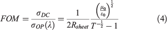
EQE of the devices was measured as a function of wavelength from 300 to 1100 nm by passing the chopped light from a xenon source through a monochromator. The transparency of the GOCNT hybrid films at 550 nm was determined by UV-vis-NIR spectroscopy (Lambda 950 PerkinElmer) with the background subtraction of a clean glass slide. The Rsheet of the GOCNT films was measured by a four-point probe in linear configuration (Keithlink). The optoelectronic properties of the hybrid films could then be evaluated with FOM, which is calculated with Eqn 3 rearranged to Eqn 4 as follows:
where μ0 is free space permeability (4π × 10−7 N A−2), ϵ0 is free space permittivity (8.854 × 10⁻¹² C2 N−1 m−2), and σOP(λ) and σDC are optical and electrical conductivity respectively.[59–61]
The thicknesses of HTL materials were measured by AFM (Multimode, Bruker). Raman spectra of the films were determined with an AFM–Raman system (Nanonics-Horiba) with an excitation energy of 1.96 eV. The morphology of the film surface was characterised by SEM (Inspect F50, FEI).
Supplementary Material
Detailed information on characterisation of the films used in different cells and cell performance as a function of film thickness and AuCl3 doping is available on the Journal’s website.
Conflicts of Interest
The authors declare no conflicts of interest.
Acknowledgements
This work was supported by the South Australian node of both the Australian Microscopy and Microanalysis Research Facility (AMMRF) and the Australian National Fabrication Facility (ANFF). H.D.P is thankful to QUT for offering a QUTPRA scholarship to conduct his research work. P.S. is thankful for financial support from the Australian Research Council (ARC) for a Future Fellowship (FT130101337) and QUT core funding (QUT/322120–0301/07). The support of the ARC Discovery Program (grant numbers DP150101354 and DP160101301) is gratefully acknowledged. Thanks to Professor David Lewis for offering PEDOT:PSS.
References
[1] V. L. Davis, S. Quaranta, C. Cavallo, A. Latini, F. Gaspari, Sol. Energy Mater. Sol. Cells 2017, 167, 162.| Crossref | GoogleScholarGoogle Scholar | 1:CAS:528:DC%2BC2sXmt1eru7Y%3D&md5=27bda863ad3715db802ce76469fe21acCAS |
[2] S. N. Habisreutinger, R. J. Nicholas, H. J. Snaith, Adv. Energy Mater. 2017, 7, 1601839.
| Crossref | GoogleScholarGoogle Scholar |
[3] F. R. Li, Y. Xu, W. Chen, S. H. Xie, J. Y. Li, J. Mater. Chem. A 2017, 5, 10374.
| Crossref | GoogleScholarGoogle Scholar | 1:CAS:528:DC%2BC2sXmsFaqtb0%3D&md5=13f0c55465f9dfba0c9ab3590b3621d8CAS |
[4] T. A. Shastry, M. C. Hersam, Adv. Energy Mater. 2017, 7, 1601205.
| Crossref | GoogleScholarGoogle Scholar |
[5] K. Aitola, K. Domanski, J. P. Correa-Baena, K. Sveinbjornsson, M. Saliba, A. Abate, M. Gratzel, E. Kauppinen, E. M. J. Johansson, W. Tress, A. Hagfeldt, G. Boschloo, Adv. Mater. 2017, 29, 1606398.
| Crossref | GoogleScholarGoogle Scholar |
[6] I. Celik, B. E. Mason, A. B. Phillips, M. J. Heben, D. Apul, Environ. Sci. Technol. 2017, 51, 4722.
| Crossref | GoogleScholarGoogle Scholar | 1:CAS:528:DC%2BC2sXjtl2rtL8%3D&md5=9ed2e90112f1969130fe3d57154ec739CAS |
[7] R. Garg, S. Elmas, T. Nann, M. R. Andersson, Adv. Energy Mater. 2017, 7, 1601393.
| Crossref | GoogleScholarGoogle Scholar |
[8] J. Ma, W. Shen, F. Yu, J. Power Sources 2017, 351, 58.
| Crossref | GoogleScholarGoogle Scholar | 1:CAS:528:DC%2BC2sXkvFalsL8%3D&md5=6664c58b8afb118fa365d82d75e001b0CAS |
[9] W. Wei, B. Y. Hu, F. M. Jin, Z. Z. Jing, Y. X. Li, A. A. G. Blanco, D. J. Stacchiola, Y. H. Hu, J. Mater. Chem. A 2017, 5, 7749.
| Crossref | GoogleScholarGoogle Scholar | 1:CAS:528:DC%2BC2sXlsV2murg%3D&md5=031fba8f58dfb6eea5763600a2c326b7CAS |
[10] K. Patel, P. K. Tyagi, Carbon 2017, 116, 744.
| Crossref | GoogleScholarGoogle Scholar | 1:CAS:528:DC%2BC2sXjsVyhsbs%3D&md5=bdd12e0ad4544b26fb869c153bdd25a4CAS |
[11] S. Tadepalli, H. Hamper, S. H. Park, S. Cao, R. R. Naik, S. Singamaneni, ACS Biomater. Sci. Eng. 2016, 2, 1084.
| Crossref | GoogleScholarGoogle Scholar | 1:CAS:528:DC%2BC28XptlOgs78%3D&md5=0d40fe66e8a3540fbfa364bc7016ef78CAS |
[12] N. D. Tissera, R. N. Wijesena, J. R. Perera, K. M. N. de Silva, G. A. J. Amaratunge, Appl. Surf. Sci. 2015, 324, 455.
| Crossref | GoogleScholarGoogle Scholar | 1:CAS:528:DC%2BC2cXhvV2ms7zE&md5=2c9758bc2416e5de7fb29e95aacbae24CAS |
[13] M. H. Wahid, X. J. Chen, C. T. Gibson, C. L. Raston, Chem. Commun. 2015, 11709.
| Crossref | GoogleScholarGoogle Scholar | 1:CAS:528:DC%2BC2MXhtVCls7jM&md5=f3a965d9a5375e24f110118d781369d5CAS |
[14] L. Yu, D. Tune, C. Shearer, J. Shapter, ChemSusChem 2015, 8, 2940.
| Crossref | GoogleScholarGoogle Scholar | 1:CAS:528:DC%2BC2MXotVClt7c%3D&md5=bd25376578d408b58e4c02c36883b87dCAS |
[15] G. Z. Sun, X. Zhang, R. Z. Lin, J. Yang, H. Zhang, P. Chen, Angew. Chem. Int. Ed. 2015, 54, 4651.
| Crossref | GoogleScholarGoogle Scholar | 1:CAS:528:DC%2BC2MXkvF2nurs%3D&md5=1089de7a61a3248b99604f273e51dddcCAS |
[16] S. Kumar, W. Ahlawat, R. Kumar, N. Dilbaghi, Biosens. Bioelectron. 2015, 70, 498.
| Crossref | GoogleScholarGoogle Scholar | 1:CAS:528:DC%2BC2MXlsVOjsbw%3D&md5=c2cd589f0f73b12c95979bc5dc9ee497CAS |
[17] L. P. Yu, D. Tune, C. Shearer, T. Grace, J. Shapter, IEEE J. Photovolt. 2016, 6, 688.
| Crossref | GoogleScholarGoogle Scholar |
[18] L. P. Yu, D. D. Tune, C. J. Shearer, J. G. Shapter, Sol. Energy 2015, 118, 592.
| Crossref | GoogleScholarGoogle Scholar | 1:CAS:528:DC%2BC2MXhtVeqsrfI&md5=aa82bd8198a7497c3ec30a04ef68a169CAS |
[19] D. D. Tune, B. S. Flavel, R. Krupke, J. G. Shapter, Adv. Energy Mater. 2012, 2, 1043.
| Crossref | GoogleScholarGoogle Scholar | 1:CAS:528:DC%2BC38XhsFags73E&md5=6216c57a9d3c593386255d5b1d6b17b9CAS |
[20] F. De Nicola, M. Salvato, C. Cirillo, M. Crivellari, M. Boscardin, M. Passacantando, M. Nardone, F. De Matteis, N. Motta, M. De Crescenzi, P. Castrucci, Carbon 2017, 114, 402.
| Crossref | GoogleScholarGoogle Scholar | 1:CAS:528:DC%2BC28XitFKrtb7M&md5=69a9195aa155f3349f93f66fbe53ee0bCAS |
[21] Y. Jia, P. X. Li, X. C. Gui, J. Q. Wei, K. L. Wang, H. W. Zhu, D. H. Wu, L. H. Zhang, A. Y. Cao, Y. Xu, Appl. Phys. Lett. 2011, 98, 133115.
| Crossref | GoogleScholarGoogle Scholar |
[22] D. D. Tune, B. S. Flavel, J. S. Quinton, A. V. Ellis, J. G. Shapter, ChemSusChem 2013, 6, 320.
| Crossref | GoogleScholarGoogle Scholar | 1:CAS:528:DC%2BC3sXosFGitg%3D%3D&md5=abfcbe1c8b0fe8fd0fc7468a736c5a51CAS |
[23] L. Yu, D. D. Tune, C. J. Shearer, J. G. Shapter, ChemNanoMat 2015, 1, 115.
| Crossref | GoogleScholarGoogle Scholar | 1:CAS:528:DC%2BC2MXhvVOmu7nE&md5=346181fa26d66ba2e65246fddc8caec4CAS |
[24] L. Yu, M. Batmunkh, T. Grace, M. Dadkhah, C. Shearer, J. Shapter, J. Mater. Chem. A 2017, 5, 8624.
| Crossref | GoogleScholarGoogle Scholar | 1:CAS:528:DC%2BC2sXmtVGiu7Y%3D&md5=51c4c275eb556b7b82f0187b3980cef3CAS |
[25] Z. Yuan, Z. Wu, S. Bai, Z. Xia, W. Xu, T. Song, H. Wu, L. Xu, J. Si, Y. Jin, B. Sun, Adv. Energy Mater. 2015, 5, 1500038.
| Crossref | GoogleScholarGoogle Scholar |
[26] A. Abrusci, S. D. Stranks, P. Docampo, H.-L. Yip, A. K. Y. Jen, H. J. Snaith, Nano Lett. 2013, 13, 3124.
| Crossref | GoogleScholarGoogle Scholar | 1:CAS:528:DC%2BC3sXpsFGlu7o%3D&md5=e6d9f405e1985ef1b939b386b948158aCAS |
[27] H.-W. Chen, T.-Y. Huang, T.-H. Chang, Y. Sanehira, C.-W. Kung, C.-W. Chu, M. Ikegami, T. Miyasaka, K.-C. Ho, Sci. Rep. 2016, 6, 34319.
| Crossref | GoogleScholarGoogle Scholar | 1:CAS:528:DC%2BC28Xhs1emsbvE&md5=152d1a259450ba4ad4a25a446406a1c1CAS |
[28] H. D. Pham, H. Hu, K. Feron, S. Manzhos, H. Wang, Y. M. Lam, P. Sonar, Solar RRL 2017, 1, 1700105.
[29] H. D. Pham, Z. Wu, L. K. Ono, S. Manzhos, K. Feron, N. Motta, Y. Qi, P. Sonar, Adv. Electronic Mater. 2017, 3, 1700139.
[30] Y. C. Li, S. R. Jia, Z. Y. Liu, X. Q. Liu, Y. Wang, Y. Cao, X. Q. Hu, C. L. Peng, Z. Li, J. Mater. Chem. A 2017, 5, 7862.
| Crossref | GoogleScholarGoogle Scholar | 1:CAS:528:DC%2BC2sXlsV2mtLY%3D&md5=8dc58fc3aaba138dbe5b7b75fd8db0edCAS |
[31] J. B. Zhang, N. Vlachopoulos, M. Jouini, M. B. Johansson, X. L. Zhang, M. K. Nazeeruddin, G. Boschloo, E. M. J. Johansson, A. Hagfeldt, Nano Energy 2016, 19, 455.
| Crossref | GoogleScholarGoogle Scholar | 1:CAS:528:DC%2BC2MXhs1elsLbF&md5=87223b1efea7fe37fd27377c79168e70CAS |
[32] C. P. Lee, C. A. Lin, T. C. Wei, M. L. Tsai, Y. Meng, C. T. Li, K. C. Ho, C. I. Wu, S. P. Lau, J. H. He, Nano Energy 2015, 18, 109.
| Crossref | GoogleScholarGoogle Scholar | 1:CAS:528:DC%2BC2MXhslSjsLbN&md5=9240c03776803b871a2f8b2e7d860cacCAS |
[33] Y. F. Lin, C. T. Li, K. C. Ho, J. Mater. Chem. A 2016, 4, 384.
| Crossref | GoogleScholarGoogle Scholar | 1:CAS:528:DC%2BC2MXhslCks7vP&md5=9a41361fb743baa6410b38ccfea6c824CAS |
[34] D. Huang, T. Goh, J. Kong, Y. F. Zheng, S. L. Zhao, Z. Xu, A. D. Taylor, Nanoscale 2017, 9, 4236.
| Crossref | GoogleScholarGoogle Scholar | 1:CAS:528:DC%2BC2sXjt1agtb0%3D&md5=3dab3246e36a66482a728dd66c768153CAS |
[35] D. Y. Liu, Y. Li, J. Y. Yuan, Q. M. Hong, G. Z. Shi, D. X. Yuan, J. Wei, C. C. Huang, J. X. Tang, M. K. Fung, J. Mater. Chem. A 2017, 5, 5701.
| Crossref | GoogleScholarGoogle Scholar | 1:CAS:528:DC%2BC2sXhslarsb8%3D&md5=1b81ac02b1691820e985b1b74af4fe36CAS |
[36] C. T. Zuo, L. M. Ding, Adv. Energy Mater. 2017, 7, 1601193.
| Crossref | GoogleScholarGoogle Scholar |
[37] E. J. Lee, J. P. Han, S. E. Jung, M. H. Choi, D. K. Moon, ACS Appl. Mater. Interfaces 2016, 8, 31791.
| Crossref | GoogleScholarGoogle Scholar | 1:CAS:528:DC%2BC28XhslWjsbjP&md5=4ff2a03c0d7ac05ced7612a738388030CAS |
[38] X. Fan, B. G. Xu, S. H. Liu, C. H. Cui, J. Z. Wang, F. Yan, ACS Appl. Mater. Interfaces 2016, 8, 14029.
| Crossref | GoogleScholarGoogle Scholar | 1:CAS:528:DC%2BC28XnvFKhs7g%3D&md5=2cd4543a257d60020b2480430abb0774CAS |
[39] Z. M. Yu, Y. J. Xia, D. H. Du, J. Y. Ouyang, ACS Appl. Mater. Interfaces 2016, 8, 11629.
| Crossref | GoogleScholarGoogle Scholar | 1:CAS:528:DC%2BC28Xms1Gqs7o%3D&md5=1444e8ddf1257048fd1da0186897aaf0CAS |
[40] B. Li, X. T. Zhang, P. Chen, X. H. Li, L. L. Wang, C. Zhang, W. T. Zheng, Y. C. Liu, RSC Adv. 2014, 4, 2404.
| Crossref | GoogleScholarGoogle Scholar | 1:CAS:528:DC%2BC3sXhvV2lt7jP&md5=03f0f6853d750766be401a4096eb17f3CAS |
[41] D. Li, M. B. Muller, S. Gilje, R. B. Kaner, G. G. Wallace, Nat. Nanotechnol. 2008, 3, 101.
| Crossref | GoogleScholarGoogle Scholar | 1:CAS:528:DC%2BD1cXhs1ajtLs%3D&md5=1f0d5a20ec04016be1c508f4db233e67CAS |
[42] R. S. Dey, S. Hajra, R. K. Sahu, C. R. Raj, M. K. Panigrahi, Chem. Commun. 2012, 787.
| Crossref | GoogleScholarGoogle Scholar |
[43] A. K. Das, M. Srivastav, R. K. Layek, M. E. Uddin, D. Jung, N. H. Kim, J. H. Lee, J. Mater. Chem. A 2014, 2, 1332.
| Crossref | GoogleScholarGoogle Scholar | 1:CAS:528:DC%2BC3sXitVShs7vM&md5=88a229ea0672d097e63e87a3de8d256fCAS |
[44] S. B. Ye, J. C. Feng, RSC Adv. 2016, 6, 39681.
| Crossref | GoogleScholarGoogle Scholar | 1:CAS:528:DC%2BC28XmsF2itLo%3D&md5=d70e26e9c19400bfd435b1ec4cd3581cCAS |
[45] D. D. Tune, J. G. Shapter, Nanomaterials 2013, 3, 655.
| Crossref | GoogleScholarGoogle Scholar |
[46] M. S. Dresselhaus, G. Dresselhaus, R. Saito, A. Jorio, Phys. Rep. 2005, 409, 47.
[47] S. D. M. Brown, A. Jorio, P. Corio, M. S. Dresselhaus, G. Dresselhaus, R. Saito, K. Kneipp, Phys. Rev. B 2001, 63, 155414.
| Crossref | GoogleScholarGoogle Scholar |
[48] A. M. Rao, P. C. Eklund, S. Bandow, A. Thess, R. E. Smalley, Nature 1997, 388, 257.
| Crossref | GoogleScholarGoogle Scholar | 1:CAS:528:DyaK2sXkslShurk%3D&md5=3966adfadd2b461cfc43e714148dc003CAS |
[49] R. Voggu, C. S. Rout, A. D. Franklin, T. S. Fisher, C. N. R. Rao, J. Phys. Chem. C 2008, 112, 13053.
| Crossref | GoogleScholarGoogle Scholar | 1:CAS:528:DC%2BD1cXpt1ygtbY%3D&md5=b87a2e751550bdac6b292f496e39fcedCAS |
[50] L. Yu, C. Shearer, J. Shapter, Chem. Rev. 2016, 116, 13413.
| Crossref | GoogleScholarGoogle Scholar | 1:CAS:528:DC%2BC28Xhs1SksrnM&md5=5e83fcd721d414df2f3a51fd87d92491CAS |
[51] S. M. Kim, K. K. Kim, Y. W. Jo, M. H. Park, S. J. Chae, D. L. Duong, C. W. Yang, J. Kong, Y. H. Lee, ACS Nano 2011, 5, 1236.
| Crossref | GoogleScholarGoogle Scholar | 1:CAS:528:DC%2BC3MXit1Crtg%3D%3D&md5=29949fe86d7ac0e1dce41bb7fbb09cebCAS |
[52] F. Wang, D. Kozawa, Y. Miyauchi, K. Hiraoka, S. Mouri, Y. Ohno, K. Matsuda, ACS Photonics 2014, 1, 360.
| Crossref | GoogleScholarGoogle Scholar | 1:CAS:528:DC%2BC2cXksF2ksbw%3D&md5=a7275da321ac7dc154608bd15554e88bCAS |
[53] H. He, X. Yu, Y. Wu, X. Mu, H. Zhu, S. Yuan, D. Yang, Nano Energy 2015, 16, 91.
| Crossref | GoogleScholarGoogle Scholar | 1:CAS:528:DC%2BC2MXhtFeisb%2FI&md5=2475ad7602f092bae774d74124d9e59eCAS |
[54] I. Puchades, C. C. Lawlor, C. M. Schauerman, A. R. Bucossi, J. E. Rossi, N. D. Cox, B. J. Landi, J. Mater. Chem. C 2015, 3, 10256.
| Crossref | GoogleScholarGoogle Scholar | 1:CAS:528:DC%2BC2MXhsVymtLbP&md5=d272ca007d436fad289ca5fa83920106CAS |
[55] X. K. Li, Y. Jung, K. Sakimoto, T. H. Goh, M. A. Reed, A. D. Taylor, Energy Environ. Sci. 2013, 6, 879.
| Crossref | GoogleScholarGoogle Scholar | 1:CAS:528:DC%2BC3sXivVGktrs%3D&md5=e7a0c245e5d8f78892bc7f1f52d9dbf9CAS |
[56] D. C. Marcano, D. V. Kosynkin, J. M. Berlin, A. Sinitskii, Z. Sun, A. Slesarev, L. B. Alemany, W. Lu, J. M. Tour, ACS Nano 2010, 4, 4806.
| Crossref | GoogleScholarGoogle Scholar | 1:CAS:528:DC%2BC3cXptFOqtrc%3D&md5=f19ffbb4b6c650abbd9fd4ef5c0aefa5CAS |
[57] L. Yu, T. Grace, M. D. Jazi, C. Shearer, J. Shapter, Solar RRL 2017, 1, 1600026.
| Crossref | GoogleScholarGoogle Scholar |
[58] J. N. Tey, X. Ho, J. Wei, Nanoscale Res. Lett. 2012, 7, 548.
| Crossref | GoogleScholarGoogle Scholar |
[59] B. Ruzicka, L. Degiorgi, R. Gaal, L. Thien-Nga, R. Bacsa, J. P. Salvetat, L. Forro, Phys. Rev. B 2000, 61, R2468.
| Crossref | GoogleScholarGoogle Scholar | 1:CAS:528:DC%2BD3cXns1Shtw%3D%3D&md5=c1f9acd21cfef67cecb548464891b527CAS |
[60] S. De, J. N. Coleman, ACS Nano 2010, 4, 2713.
| Crossref | GoogleScholarGoogle Scholar | 1:CAS:528:DC%2BC3cXksFeqtbY%3D&md5=f062043ae4c45bd1b2faed1c7bbc1afbCAS |
[61] L. Hu, D. S. Hecht, G. Grüner, Nano Lett. 2004, 4, 2513.
| Crossref | GoogleScholarGoogle Scholar | 1:CAS:528:DC%2BD2cXoslCqsLw%3D&md5=ac1a45bec2b2a10a5aba21e7de3fc3f1CAS |
* Joe Shapter was awarded the 2016 RACI Fensham Medal for Outstanding Contribution to Chemical Education.