
Towards ‘Computer-on-a-Particle’ Devices: Optoelectronic 1:2 Demultiplexer Based on Nanostructured Cadmium Sulfide
Agnieszka Podborska A and Konrad Szaciłowski A B CA Uniwersytet Jagielloński, Wydział Chemii, ul. Ingardena 3, 30-060 Kraków, Poland.
B Akademia Górniczo-Hutnicza, Wydział Metali Nieżelaznych, al. Mickiewicza 30, 30-059 Kraków, Poland.
C Corresponding author. Email: szacilow@agh.edu.pl; szacilow@chemia.uj.edu.pl
Australian Journal of Chemistry 63(2) 165-168 https://doi.org/10.1071/CH09440
Submitted: 28 August 2009 Accepted: 27 September 2009 Published: 26 February 2010
Abstract
Nanocrystalline sulfur-doped cadmium sulfide (CdS) prepared by microwave synthesis was investigated. Photoelectrochemical and optical characteristics of sulfur-doped CdS exhibit the photoelectrochemical photocurrent switching effect. Depending on the wavelength and applied bias, the anodic and/or cathodic photocurrent was observed. The unusual behaviour of nanocrystalline CdS allowed the construction of a combinatorial logic system from this material.
The idea of small, ubiquitous, and autonomous computing devices was first presented by Kristof Pister in 1997.[1] These devices, usually called ‘smart dust’, were supposed to be small (~1 mm3) electronic devices able to sense the environment and communicate with other devices and with the user. This idea was further developed and various sensing and labelling nanostructures became available,[2,3] and finally achieved the complexity of ‘laboratory-on-a-particle’ via integration of nanoparticles with functional biomolecules.[4–8] Apart from sensing applications, similar concepts were applied in construction of simple logic devices based on micellar and liposomic structures with embedded molecular sensors, switches, and logic gates.[9–11]
While molecular logic gates are quite ubiquitous devices, more complex molecular scale computing devices are rare.[12] Only recently some molecular devices for data transmission,[13] multiplexing,[14,15] demultiplexing,[15–17] and encoding[18–20] have been reported, none of which was based on easily available homogeneous material suitable for integration with conventional electronics.
The photoelectrochemical properties of surface-modified, wide-bandgap semiconductors have been applied to construction of prototypical logic gates and other devices, including programmable ones.[21,22] These materials proved to be suitable for construction of demultiplexers as well.[23–25]
Recently it was found that bulk modified cadmium sulfide (CdS) also presents photoelectrochemical photocurrent switching (PEPS) phenomena.[26] This material was obtained in high yield via microwave-induced hydrolysis of cadmium-thiourea complexes. Nanoparticles thus prepared, of 5–7 nm diameter, are only weakly aggregated and can be used for fabrication of photoelectrodes. Energy dispersive X-ray analysis (EDX) indicates that these samples contain an excess of sulfur over cadmium. However, XRD analysis indicated that the only phases are cubic and hexagonal CdS. This indicates the presence of excess sulfur as interstitial inclusions or thin amorphous layers. A high excess of sulfur cannot be associated with thiourea-derived surface modification, as the content of nitrogen and carbon is low, independent of the excess of thiourea. Quantum-chemical modelling of small, sulfur-doped CdS clusters indicated, that the dopant-associated energy levels are localized just below the lower edge of the conduction band.[26]
Sulfur-doped nanocrystalline CdS photoelectrodes generate photocurrents within their whole absorption spectra, including the fundamental transition and Urbach tail. The latter can be attributed to the population of intrabandgap states associated with doping sulfur atoms.[26] Polarity of the photocurrent generated at nanocrystalline CdS electrodes depends both on the photoelectrode potential and incident light wavelength. At potentials significantly higher than the band edge potential, only anodic photocurrents are observed within the whole absorption spectrum of the semiconductor (Fig. 1a). Electrons from the conduction band are transferred to the conducting support, whereas holes in the valence band are neutralized by electrons from the occupied surface state (surface SH groups). In the absence of a proper redox electrolyte (e.g. sulfide or thiols), prolonged illumination leads to photocorrosion of the material. This phenomenon is typical for all n-type semiconductors. Surprisingly, when the potential is lower than the potential of the sulfur-associated surface state, the polarity of photocurrent changes, and only cathodic photocurrents are observed (Fig. 1b). This effect is associated with contribution of the interstitial sulfur atoms in the photoinduced interfacial electron transfer process: conduction band electrons are trapped at shallow traps (associated with extra sulfur centres), and are subsequently transferred to oxygen molecules present in the electrolyte (Fig. 2). The reverse process (generation of anodic photocurrent) is thermodynamically disfavoured. Furthermore, within a very narrow potential window, illumination with low energy light (just below the bandgap energy, i.e. within the Urbach tail) results in a photocathodic response, whereas more energetic light induces photoanodic response (Fig. 1c). This light-induced photocurrent switching also results from contribution of dopant levels in the electron transfer processes. Sulfur-centred intrabandgap states are directly populated via optical excitation within the Urbach tail, whereas the conduction band is populated during excitation within the fundamental transition.[26]

|

|
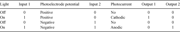
Proper assignment of input and output data allows using these CdS nanoparticles as complex logic devices with optical and electric inputs and electric output. Two distinctly different input channels can be defined in the systems based on semiconducting photoelectrodes: optical and electrical. In the optical input the simplest and most natural signal assignment is logical ‘0’ to the dark state, and logical ‘1’ with the light source on. In the case of electric channel the assignments of the inputs can be arbitrary: ‘0’ can be assigned to anodic polarization and ‘1’ to cathodic one or vice versa. In the case of photocurrent switching phenomena, i.e. when both polarities of photocurrent are allowed, it is convenient to split the electric output into two channels, one associated with anodic photocurrent, and the other with the cathodic one.
When the above signal assignments are applied to the CdS photoelectrodes, they behave as optoelectronic two-channel demultiplexers. These devices collect information in the form of light pulses, whereas photoelectrode potential can be regarded as addressing input. The generated photocurrent changes its polarity according to the photoelectrode potential, i.e. input signals are directed to anodic or cathodic output channels (Table 1). Real demultiplexing can be achieved when photoelectrodes are coupled with two diodes discriminating photocurrent polarities.
|
The system converts light pulses into electric signals and, depending on the polarization of the photoelectrode polarity of the resulting electric pulses changes accordingly. Furthermore, as the switching process (in contrary to the surface-modified TiO2-based systems)[21–23] does not involve net electrochemical reactions (but is based on tuning of electron transfer energetics), the devices should operate reversibly at much higher rates.
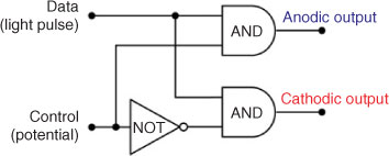
Thus, a signal applied to the data input is always transmitted by one of the AND gates (see Fig. 3) and directed into one of the output channels. Therefore, the sulfur-doped cadmium sulfide nanoparticles can serve as simple two-channel optoelectronic demultiplexers. This is an interesting example of a simple chemical system behaving as a complex electronic circuit consisting of three logic elements.
|
The most interesting feature of this material lies in the complexity of electronic functions when contrasted with its relatively simple molecular structure. Sulfur-doped nanoparticles behave as 1:2 demultiplexers irrespectively of their size and morphology. Furthermore, no electronic interaction between individual particles is needed for this operation. Thus even single nanoparticle of 5 nm diameter can be regarded as a complex logic device with functionality described by a circuit consisting of three logic gates (Fig. 3). Therefore, these CdS-based devices can compete, at least as dimensions are taken into account, with the smallest electronic devices ever created: SketchFETs[27] and graphene transistors,[28] as one nanoparticle, which occupies a surface of only 25 nm2 performs like a complex electronic circuit. Therefore, the CdS-based optoelectronic devices can be compared with complex single nanotube devices.[29,30] Furthermore, these devices can compete with most of the reported molecular logic devices in terms of chemical complexity and interfacing feasibility. This and related materials may open a new field of nanoelectronics: instead of complex circuitry it may be enough to design a proper nanoscale material of desired performance.
Experimental
Materials
CdS samples were prepared via microwave heating of propylene glycol (45 mL) solutions of cadmium acetate hexahydrate (1 g) with ethanolamine (5 mL) as a complexing agent and thiourea (5.7 g) under a reflux condenser. Synthesis was performed in a microwave reactor constructed on the basis of the microwave oven Samsung MW87L (Samsung, Thailand). Products were separated by centrifugation, washed with a large volume of water and vacuum-dried at room temperature. All reagents were supplied by Fluka (Switzerland).
Preparation of Photoelectrode
Working electrodes were prepared on indium tin oxide (Aldrich). Films were deposited from aqueous suspensions of semiconducting powders via a cast coating technique. Films were dried with a stream of hot air and used for measurement immediately after preparation.
Instrumentation
Energy dispersion X-ray (EDX) analysis was performed on an EDX Quantax 200 spectrometer with an XFlash 4010 detector (Bruker AXS) operating at 25 kV. Diffuse reflectance spectra were recorded on a Lambda 12 (Perkin–Elmer, USA) spectrophotometer equipped with a 5 cm integration sphere. Barium sulfate of spectral purity was used as a reference material. Photoelectrochemical measurements were performed on a BAS CV-50W electrochemical analyzer (Bioanalytical Systems, USA), and an aqueous 0.1 M KNO3 solution was used as an electrolyte. Photocurrents were recorded using a classical three-electrode setup with a platinum wire counter electrode and a Ag/AgCl reference electrode.
Acknowledgements
Authors thank Dr. Iwona B. Szymańska for performance of EXD analyses and Professor Dr. Jeremiasz K. Jeszka for fruitful discussions. Financial support from Polish Ministry of Science and Higher Education (grant No. 1609/B/H03/2009/36) is also acknowledged.
[1]
B. Warneke,
M. Last,
B. Liebowitz,
K. S. J. Pister,
Computer 1997, 34, 2.
| Crossref | GoogleScholarGoogle Scholar |
CAS |
| Crossref | GoogleScholarGoogle Scholar |
CAS |
| Crossref | GoogleScholarGoogle Scholar |
CAS |
| Crossref | GoogleScholarGoogle Scholar |
CAS |
| Crossref | GoogleScholarGoogle Scholar |
CAS |
| Crossref | GoogleScholarGoogle Scholar |
CAS |
| Crossref | GoogleScholarGoogle Scholar |
CAS |
| Crossref | GoogleScholarGoogle Scholar |
CAS |
| Crossref | GoogleScholarGoogle Scholar |
CAS |
| Crossref | GoogleScholarGoogle Scholar |
CAS |
| Crossref | GoogleScholarGoogle Scholar |
| Crossref | GoogleScholarGoogle Scholar |
CAS |
| Crossref | GoogleScholarGoogle Scholar |
| Crossref | GoogleScholarGoogle Scholar |
CAS |
| Crossref | GoogleScholarGoogle Scholar |
| Crossref | GoogleScholarGoogle Scholar |
CAS |
| Crossref | GoogleScholarGoogle Scholar |
CAS |
| Crossref | GoogleScholarGoogle Scholar |
CAS |
| Crossref | GoogleScholarGoogle Scholar |
| Crossref | GoogleScholarGoogle Scholar |
| Crossref | GoogleScholarGoogle Scholar |
| Crossref | GoogleScholarGoogle Scholar |
| Crossref | GoogleScholarGoogle Scholar |
CAS |
| Crossref | GoogleScholarGoogle Scholar |
| Crossref | GoogleScholarGoogle Scholar |
CAS |
| Crossref | GoogleScholarGoogle Scholar |
CAS |
| Crossref | GoogleScholarGoogle Scholar |
CAS |
| Crossref | GoogleScholarGoogle Scholar |
CAS |
| Crossref | GoogleScholarGoogle Scholar |
CAS |
