

Enhanced Water Splitting on Thin-film Hematite Photoanodes Functionalized with Lithographically Fabricated Au Nanoparticles
Beniamino Iandolo A B and Michael Zäch AA Department of Applied Physics, Division for Chemical Physics, Chalmers University of Technology, 412 96 Göteborg, Sweden.
B Corresponding author. Email: iandolo@chalmers.se
Australian Journal of Chemistry 65(6) 633-637 https://doi.org/10.1071/CH11453
Submitted: 1 December 2011 Accepted: 4 April 2012 Published: 21 June 2012
Abstract
Iron oxide in its crystalline form (hematite, α-Fe2O3) is an interesting candidate as a photoanode material for photoelectrochemical cells, in spite of its non-optimal optoelectronic properties. We report here on the beneficial effect of Au nanodisks on the photocurrent of α-Fe2O3. Photoanodes consisting of ultra-thin α-Fe2O3 films lithographically functionalized with Au nanodisks of varying size were characterized and tested. We found a significant increase in photocurrent for the functionalized samples. The highest increase in incident photon-to-electron conversion efficiency is roughly one order of magnitude compared with a reference sample without Au nanodisks and was found for incident light of 420 nm in wavelength. A detailed understanding of the phenomena underlying such an increase in efficiency is crucial to fully exploit the beneficial effect of the metallic nanostructures. This would contribute to make Fe2O3 more competitive in the race for the development of a commercially viable device for water splitting.
Introduction
Efficient and sustainable large-scale production of chemical fuels through energy coming from the sun is an attractive option to address the global energy challenge. In particular, hydrogen has the potential to replace fossil fuels as our energy backbone in a long-term perspective.[1] Light-driven water splitting has been an appealing possibility towards clean hydrogen production ever since the pioneering work of Fujishima and Honda.[2] A distinction is typically made between molecular and photochemical (photocatalytic and photoelectrochemical (PEC)) approaches to water splitting. In the former case, light harvesting occurs in macromolecular complexes, and donor and acceptor complexes are used to separate excited electrons and holes and to run H2 and O2 evolution reactions with these excited charge carriers, respectively.[3,4] In the latter case, light is absorbed in a semiconductor generating electron-hole pairs. Once electrons and holes are separated, they take part in H2 and O2 evolution, respectively, either in close proximity to one another in the case of photocatalytic water splitting or at macroscopically different locations in a PEC cell. Intensive research is ongoing towards the development of catalysts and light absorbing materials that satisfy all the requirements – in terms of energy conversion efficiency, costs and safety – to make water splitting commercially viable.[5] Recent findings regarding all approaches mentioned above have been discussed at the Global Artificial Photosynthesis conference organized by Professor T. Faunce and held in August 2011 on Lord Howe Island, Australia.
Concerning PEC water splitting, hematite (α-Fe2O3) has emerged from >200 tested compounds[6] as an appealing candidate to be used as a photoanode. Fe2O3 is a non-toxic, inexpensive, abundant and photo-stable semiconductor capable of absorbing two thirds of the visible light owing to its bandgap of 2.0 eV.[7] However, its solar-to-chemical energy conversion efficiency remains relatively low,[8] mainly due to an intrinsic conflict between light absorption and charge transport properties. Fe2O3* is an n-type semiconductor characterized by poor electrical conductivity[7,8] and an extremely short hole diffusion length of around 4 nm.[9,10] This implies that only holes that are generated within a very short distance from the semiconductor-electrolyte interface avoid recombination and reach the surface where they take part into the water oxidation reaction. In contrast, the absorption of visible light in hematite requires a comparably large amount of material (the absorption length, i.e. the thickness required to absorb 63 % of the incoming light, is 118 nm for a photon with energy of 2.26 eV,[11] which corresponds to a wavelength of ~550 nm).
Metallic nanostructures have already proven to increase the performance of solid-state and dye-sensitized solar cells,[12,13] as well as the photocurrent of PEC cells.[14–16] In previous work, an enhancement in photocurrent in hematite functionalized with Au nanostructures was found in the wavelength region where such nanostructures support (localized) surface plasmon resonances, or (L)SPR. The enhanced electric fields around the nanostructures and the increased light absorption in Fe2O3 due to scattering by the Au were accounted for the observed changes in photocurrent.[15–17] However, several (other) possible mechanisms of increasing photocurrent in PEC cells upon functionalization with metallic nanostructures have been outlined in a recent review.[18]
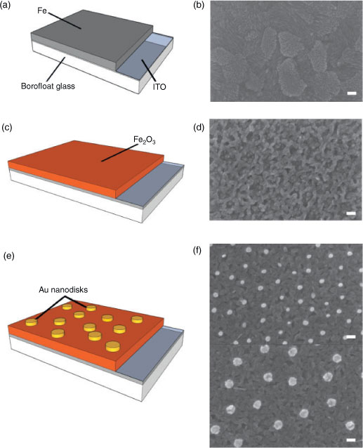
In this Communication, we report on our observation of a significant increase in incident photon-to-current efficiency (IPCE) in Fe2O3 photoanodes functionalized with Au nanodisks, in a wavelength region far from the LSPR in the Au nanodisks. In particular, we tested simple and reproducible model systems based on ultra-thin Fe2O3 films, for which bulk electron-hole recombination is not a major limiting factor. For a detailed description of the fabrication procedure, the reader is referred to the Supplementary Material. In brief, we fabricated Fe2O3 films by thermal oxidation of Fe deposited by electron-beam evaporation on top of indium tin oxide (ITO)-coated glass. Then we functionalized the Fe2O3 films with Au nanodisks via hole-mask colloidal lithography. We focussed on Au nanodisks of various diameters, while keeping constant the disk height and surface coverage. Hole-mask colloidal lithography allows fast fabrication of random nanoparticle arrangements of various metals with different shapes in a wide size range, covering relatively large areas (i.e. a few cm2).[19] The use of such a technique is new in this context, and is suitable for systematic studies of the influence of metallic nanoparticles due to its simplicity, tunability and versatility. We have chosen Au for our nanodisks in view of several favourable properties, including (i) proven stability under the operation conditions in a PEC cell and (ii) tunability of the LSPR peak position by appropriate choice of nanodisk size. In particular, nanodisks can be manufactured so that the LSPR peak lies in the region of poor absorption in Fe2O3,[20] which can be of interest in view of maximizing plasmon-related beneficial effects.
Results and Discussion
The as-fabricated iron oxide films are compact, as seen from the top-view SEM image shown in Fig. 1d, and have a roughness similar to that of the underlying 120 nm-thick ITO charge collectors (for atomic force microscopy height images, see Fig. S1 in the Supplementary Material).
|
All peaks in the X-ray diffraction spectra (see Fig. S2 in the Supplementary Material) can be assigned to Fe2O3 (JCPDS 33-0664) or ITO (JCPDS 06-0416), confirming that the films are composed of polycrystalline Fe2O3. One notices the presence of two preferred crystal orientations in Fe2O3, namely the [104] and the [110] directions, in agreement with previous studies on Fe2O3 thin films deposited on top of ITO.[21]
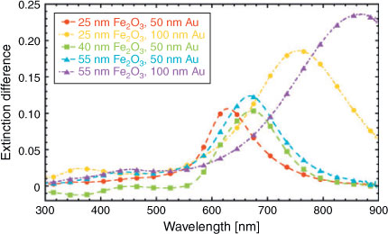
Light extinction was measured in water for the functionalized samples and for reference samples consisting of Fe2O3 of the respective same thickness.
Fig. 2 shows the extinction difference spectra between functionalized and non-functionalized samples, i.e. ΔE ≡ EFe2O3+Au – EFe2O3. All the ΔE spectra show one peak, which corresponds to the presence of LSPR in the Au nanodisks.
|
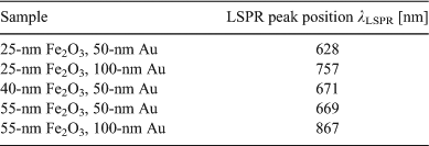
Table 1 summarizes the position of the ΔE peaks for different samples. Two trends are distinguishable: first, increasing the disk diameter from 50 to 100 nm causes a redshift (i.e. shift to longer wavelengths) of the ΔE peak. In general, such a redshift is expected for increasing nanodisk diameter and is well understood in terms of dynamic depolarization of the nanodisk.[22] Second, increasing the Fe2O3 thickness for a given Au nanodisk diameter also results in a redshift of the ΔE peak. The change in nanoenvironment around the nanodisks accounts for the redshift; with the Fe2O3 thickness increasing from 25 to 40 nm, the Au disks are surrounded by a medium whose effective refractive index neff increases because Fe2O3 has a higher refractive index than ITO in the spectral region of interest.[23] Such an increase in neff results in the observed redshift of the ΔE peaks. Upon further increasing the Fe2O3 thickness to 55 nm, however, we see no further redshift. This observation can be qualitatively understood by recalling that LSPR are sensitive to changes in the refractive index of the surrounding medium only within a certain volume.[24]
|
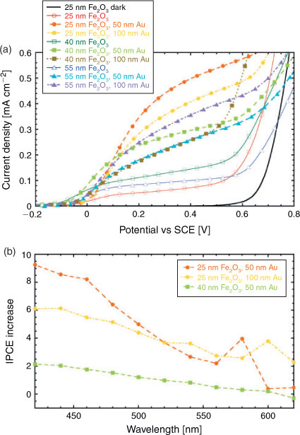
Fig. 3a shows the photocurrent – measured under white light illumination in 1 M KOH (pH 13.5) – of samples with different Fe2O3 thickness and Au nanodisk diameter. Further details regarding the test procedure, as well as the reproducibility of the measurements, are given in the Supplementary Material. First, we notice that the photocurrent of the bare Fe2O3 samples depends on the film thickness, with the 40 nm-thick film showing the highest photocurrent and lowest onset potential values (for the latter, see Fig. S3 in the Supplementary Material). Such intermediate thickness guarantees an optimal compromise between light absorption and charge transport for this film structure. This behaviour is characteristic of Fe2O3 compact thin films and has been observed previously.[25]
|
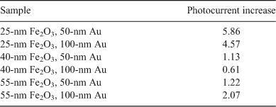
All the functionalized samples show an increase in photocurrent as compared to a bare Fe2O3 sample with the same thickness over the whole considered potential window. Table 2 summarizes the photocurrent increase, defined here as (photocurrent of functionalized sample – photocurrent of reference sample)/(photocurrent of reference sample), measured at 0.223 V against the saturated calomel reference electrode (which corresponds to 1.23 V against the standard hydrogen electrode at pH 13.5). The 25-nm Fe2O3 samples show not only the highest relative increase in photocurrent (of roughly a factor of six), but also the highest photocurrent in absolute terms. A beneficial effect of nanostructures of various metals (Au,[17] Ti[26] and even Zn[27]) on the onset potential for the photocurrent has been reported previously. Catalytic activity of the metal has then been accounted for such influence. In our case, however, we do not see a dramatic shift of the onset potential upon functionalization with Au nanodisks (see Fig. S3 in the Supplementary Material for details).
|
The response of the films to monochromatic light is a key to gain insight in the mechanisms responsible for the increase in photocurrent. Fig. 3b shows the increase in IPCE, defined in an analogous way as previously for the photocurrent increase, for a few representative samples.
The 25-nm Fe2O3 films show a higher IPCE increase than the 40-nm Fe2O3 film over the entire investigated wavelength range. This is consistent with the white light photocurrent-voltage measurements discussed above. We notice that the 25-nm Fe2O3 films are characterized by a local maximum in the IPCE increase close to the wavelength corresponding to the bandgap in Fe2O3. Such relative maxima are in the region of enhanced light extinction due to LSPR in the Au nanodisks. For both samples, we attribute this relative maximum in IPCE increase to the plasmonic activity of the Au nanodisks. An increase in IPCE upon functionalization with Au nanostructures in the spectral region of plasmonic activity of the Au is expected and has been recently demonstrated.[15–17] Remarkably, we observe the highest IPCE increase in our samples for the shortest wavelengths in the measurement range, between 420 and 460 nm. In this part of the visible spectrum, however, there is no clear difference in optical extinction between functionalized and reference samples. Hot electron transfer, electric field enhancement, and increased absorption due to enhanced light scattering cannot account for the observed IPCE increase in this region since plasmonic resonances are not active here. Nonetheless, we observe here the greatest improvement in IPCE, with a remarkable maximum value of 9.2 for the 25-nm hematite film functionalized with 50-nm Au disks at 420 nm. To the best of our knowledge, this is the first observation of such a pronounced effect in Fe2O3 films functionalized with metallic nanostructures. Considering that there is essentially no overlap with the region of increased optical extinction, we speculate that this IPCE increase is caused by a Schottky barrier at the semiconductor-metal interface that improves charge separation. The possibility of beneficial effects due to such a mechanism has been hypothesized in a recent review.[18] At present, the validity of this hypothesis is yet to be verified in our model system and is therefore the subject of current investigation.
Conclusions
In conclusion, we demonstrated that Au nanodisks deposited by hole-mask colloidal lithography enhance the photocurrent in dense, polycrystalline ultra-thin Fe2O3 films. The increase in photocurrent under white light illumination is up to a factor of six for a 25-nm thin Fe2O3 film functionalized with 50-nm Au nanodisks. The relative maximum in IPCE increase close to the bandgap energy in Fe2O3 overlaps with the region of increased light extinction in the Au-functionalized samples. Therefore, we attribute such an increase in IPCE to LSPR-induced phenomena. We observed a much higher increase in IPCE for shorter wavelengths, up to an order of magnitude (for a 25-nm thin Fe2O3 film functionalized with 50-nm Au nanodisks), where no significant light extinction difference is caused by the Au nanodisks.
We tentatively attribute this enhancement in IPCE to a Schottky barrier at the semiconductor–metal interface, which results in improved charge separation. Further investigations are ongoing in order to verify this hypothesis. The effect of varying other parameters in this model system, such as sample geometry (for instance, Au nanodisks embedded in Fe2O3) and surface coverage of the Au nanodisks on the photocurrent in Fe2O3 should be considered. In this regard, it is worth noting that the very small surface coverage (i.e. small amount of Au) used in this work is favourable in view of issues related to availability and cost of Au. We anticipate that a combined effort in all these directions would lead to an optimized Fe2O3 : Au nanoparticle system where the beneficial effect of the metallic nanostructures is fully exploited. This would make Fe2O3 even more competitive in the race for the development of a commercially viable device for water splitting. The main competitive advantages of iron oxide as compared to molecular approaches are its low cost, its high stability, its large abundance and its potentially high solar-to-hydrogen conversion efficiency, with no need to separate hydrogen and oxygen. Iron oxide is furthermore an interesting alternative to silicon, which is currently used as photovoltaic material in Reece et al.’s artificial leaf, since it may make the device even cheaper to produce.
Supplementary Material
Details about sample fabrication and characterization (atomic force microscopy and X-ray diffraction scans) and measurements of photocurrent onset potential and of photocurrent in control samples are available on the Journal’s website.
Acknowledgments
We gratefully acknowledge V. Langer for the XRD measurements, R. Martins for the help with the photoelectrochemical setup and the Swedish Energy Agency (project no 32078-1) for financial support.
References
[1] US Department of Energy, Basic research needs for solar energy utilization (report) 2005.[2] A. Fujishima, K. Honda, Nature 1972, 238, 37.
| Crossref | GoogleScholarGoogle Scholar | 1:CAS:528:DyaE38XltVykurw%3D&md5=03d07b9827056cfb43c8159c90239687CAS |
[3] S. Y. Reece, J. A. Hamel, K. Sung, T. D. Jarvi, A. J. Esswein, J. J. H. Pijpers, D. G. Nocera, Science 2011, 334, 645.
| Crossref | GoogleScholarGoogle Scholar | 1:CAS:528:DC%2BC3MXhtlyqu7vF&md5=e0298161b92e218b9b45c56538dc6eb5CAS |
[4] G. C. Dismukes, R. Brimblecombe, G. A. N. Felton, R. S. Pryadun, J. E. Sheats, L. Spiccia, G. F. Swiegers, Acc. Chem. Res. 2009, 42, 1935.
| Crossref | GoogleScholarGoogle Scholar | 1:CAS:528:DC%2BD1MXhsVSgtb%2FL&md5=7ee1e63bbf20e924e0a4d165bd1f212dCAS |
[5] US Department of Energy, Interim update document (report) 2011.
[6] F. E. Osterloh, Chem. Mater. 2008, 20, 35.
| Crossref | GoogleScholarGoogle Scholar | 1:CAS:528:DC%2BD2sXhsVWqsL3E&md5=9ea2398a70b48b0126639f609bbf7158CAS |
[7] R. M. Cornell, U. Schwertmann, The Iron Oxides 2003 (Wiley, USA).
[8] J. A. Glasscock, P. R. F. Barnes, I. C. Plumb, A. Bendavid, P. J. Martin, Thin Solid Films 2008, 516, 1716.
| Crossref | GoogleScholarGoogle Scholar | 1:CAS:528:DC%2BD1cXhsVGnsLY%3D&md5=cc382e4a64b3d04c206c6db428980999CAS |
[9] K. Sivula, F. Le Formal, M. Grätzel, ChemSusChem 2011, 4, 432.
| Crossref | GoogleScholarGoogle Scholar | 1:CAS:528:DC%2BC3MXks1WktLY%3D&md5=2d427f9baccfe01e0c406edebe721136CAS |
[10] J. H. Kennedy, K. W. Frese, Electrochem. Soc. 1978, 125, 709.
| Crossref | GoogleScholarGoogle Scholar | 1:CAS:528:DyaE1cXktFCksb8%3D&md5=2af9e54531d8b61833c224aecb0ac2ebCAS |
[11] I. Balberg, H. L. Pinch, J. Magn. Magn. Mater. 1978, 7, 12.
| Crossref | GoogleScholarGoogle Scholar |
[12] H. A. Atwater, A. Polman, Nat. Mater. 2010, 9, 205.[and references therein]
| Crossref | GoogleScholarGoogle Scholar | 1:CAS:528:DC%2BC3cXitFGltbg%3D&md5=b7be45c5487707b341bc0e93ae9bf69eCAS |
[13] S. Linic, P. Christopher, D. B. Ingram, Nat. Mater. 2011, 10, 911.[and references therein]
| Crossref | GoogleScholarGoogle Scholar | 1:CAS:528:DC%2BC3MXhsFWqtb%2FO&md5=1ed74e57657948db6b0a8ce77ada7d5fCAS |
[14] Y. Tian, T. Tatsuma, J. Am. Chem. Soc. 2005, 127, 7633.
[15] H. Gao, C. Liu, H. E. Jeong, P. Yang, ACS Nano 2012, 6, 234.
| Crossref | GoogleScholarGoogle Scholar | 1:CAS:528:DC%2BC3MXhsFOht7%2FJ&md5=65c8828b4405905d17fcced993c89320CAS |
[16] I. Thomann, B. A. Pinaud, Z. Chen, B. M. Clemens, T. F. Jaramillo, M. L. Brongersma, Nano Lett. 2011, 11, 3440.
| Crossref | GoogleScholarGoogle Scholar | 1:CAS:528:DC%2BC3MXovFKkt70%3D&md5=5d825fc075df0e5e935adabce03e78d9CAS |
[17] E. Thimsen, F. Le Formal, M. Grätzel, S. C. Warren, Nano Lett. 2011, 11, 35.
| Crossref | GoogleScholarGoogle Scholar | 1:CAS:528:DC%2BC3cXhsFakur%2FI&md5=55f3a0bf86576ac35ebaacaed802c2edCAS |
[18] S. C. Warren, E. Thimsen, Energy, Environ. Sci. 2012, 5, 5133.
| Crossref | GoogleScholarGoogle Scholar | 1:CAS:528:DC%2BC3MXhs1CgsbvK&md5=3e55620753bb3bf626d8082b8500db80CAS |
[19] H. Fredriksson, Y. Alaverdyan, A. Dmitriev, C. Langhammer, D. S. Sutherland, M. Zäch, B. Kasemo, Adv. Mater. 2007, 19, 4297.
| Crossref | GoogleScholarGoogle Scholar | 1:CAS:528:DC%2BD1cXlsVY%3D&md5=e254571b13b65d4d10ce0ef069435418CAS |
[20] I. Zoric, M. Zäch, B. Kasemo, C. Langhammer, ACS Nano 2011, 5, 2535.
| Crossref | GoogleScholarGoogle Scholar | 1:CAS:528:DC%2BC3MXktFensr0%3D&md5=00d019570f8160661c337f3cf9cc3430CAS |
[21] J. D. Desai, H. M. Pathon, S.-K. Min, K.-D. Jung, O.-S. Joo, Semicond. Sci. Technol. 2005, 20, 705.
| Crossref | GoogleScholarGoogle Scholar | 1:CAS:528:DC%2BD2MXpsFKgtL8%3D&md5=88e285fad07accdb4e6a1068e33ed221CAS |
[22] K. Meier, A. Wokaun, Opt. Lett. 1983, 8, 581.
| Crossref | GoogleScholarGoogle Scholar | 1:CAS:528:DyaL3sXmt1Whtrs%3D&md5=251f0fff03706066c0656f43a6aa2b25CAS |
[23] E. W. Palik, Handbook of optical constants of solids 1991 (Academic Press: USA).
[24] T. Rindzevicius, Y. Alaverdyan, W. A. Murray, W. L. Barnes, M. Käll, J. Phys. Chem. C 2007, 111, 11806.
| Crossref | GoogleScholarGoogle Scholar | 1:CAS:528:DC%2BD2sXnvFOltL0%3D&md5=547d7ba4c5acdc2729565c856c77968fCAS |
[25] P. Hiralal, S. Saremi-Yarahmadi, B. C. Bayer, H. Wang, S. Hofmann, K. G. Upul Wijayantha, G. A. J. Amaratunga, Sol. Energy Mater. 2011, 95, 1819.
| Crossref | GoogleScholarGoogle Scholar | 1:CAS:528:DC%2BC3MXltFamurY%3D&md5=29b2873522f71404fde216cc47577578CAS |
[26] A. Kleiman-Shwarsctein, M. N. Huda, A. Walsh, Y. Yan, G. D. Stucky, Y.-S. Hu, M. M. Al-Jassim, E. W. McFarland, Chem. Mater. 2010, 22, 510.
| Crossref | GoogleScholarGoogle Scholar | 1:CAS:528:DC%2BD1MXhs1aksrvM&md5=7c0070c8365d676381da6f8545ca7be0CAS |
[27] S. Kumari, A. P. Singh, C. Tripathi, D. Chauhan, S. Dass, R. Shrivastav, V. Gupta, K. Sreenivas, V. R. Satsangi, Int. J. Phot. 2007, 2007,
* The prefix is omitted hereinafter for simplicity.