
Overcoming the Challenges of Hydrogenation in Silicon Solar Cells*
Brett J. Hallam A C , Alison M. Ciesla A , Catherine C. Chan A , Anastasia Soeriyadi A , Shaoyang Liu A , Arman Mahboubi Soufiani A , Matthew Wright A and Stuart Wenham A BA School of Photovoltaic and Renewable Energy Engineering, University of New South Wales, Sydney, NSW 2052, Australia.
B Deceased.
C Corresponding author. Email: brett.hallam@unsw.edu.au
Australian Journal of Chemistry 71(10) 743-752 https://doi.org/10.1071/CH18271
Submitted: 2 June 2018 Accepted: 24 August 2018 Published: 19 September 2018
Journal Compilation © CSIRO 2018 Open Access CC BY-NC-ND
Abstract
The challenges of passivating defects in silicon solar cells using hydrogen atoms are discussed. Atomic hydrogen is naturally incorporated into conventional silicon solar cells through the deposition of hydrogen-containing dielectric layers and the metallisation firing process. The firing process can readily passivate certain structural defects such as grain boundaries. However, the standard hydrogenation processes are ineffective at passivating numerous defects in silicon solar cells. This difficulty can be attributed to the atomic hydrogen naturally occupying low-mobility and low-reactivity charge states, or the thermal dissociation of hydrogen–defect complexes. The concentration of the highly mobile and reactive neutral-charge state of atomic hydrogen can be enhanced using excess carriers generated by light. Additional low-temperature hydrogenation processes implemented after the conventional fast-firing hydrogenation process are shown to improve the passivation of difficult structural defects. For process-induced defects, careful attention must be paid to the process sequence to ensure that a hydrogenation process is included after the defects are introduced into the device. Defects such as oxygen precipitates that form during high-temperature diffusion and oxidation processes can be passivated during the subsequent dielectric deposition and high-temperature firing process. However, for laser-based processes performed after firing, an additional hydrogenation process should be included after the introduction of the defects. Carrier-induced defects are even more challenging to passivate, and advanced hydrogenation methods incorporating minority carrier injection must be used to induce defect formation first, and, second, provide charge state manipulation to enable passivation. Doing so can increase the performance of industrial p-type Czochralski solar cells by 1.1 % absolute when using a new commercially available laser-based advanced hydrogenation tool.
Industrial Silicon Solar Cells
Over 90 % of the world’s solar cells are made using crystalline silicon – essentially purified sand.[1] After the purification process, the silicon is grown as either single crystal using the Czochralski process or as lower-quality multicrystalline by a casting process. Both of these are typically made using p-type silicon with boron doping of the order of 1 × 1016 cm−3, compared with the density of silicon atoms at 5 × 1022 cm−3. However, both crystallisation methods can introduce several impurities (including oxygen, carbon, and transition metals) as well as structural defects (including vacancies, grain boundaries, and dislocations) into the silicon lattice that form recombination-active defects in the device and reduce performance.
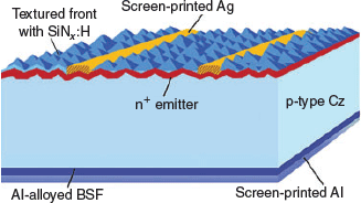
After slicing, the silicon wafer goes through the cell fabrication process. The current technology dominating the market uses a full-area aluminium back-surface-field (see Fig. 1). First, texturing of the surface is performed to reduce reflection, followed by cleaning in a mixture of HCl and HF to remove metals, followed by a dilute HF dip to remove oxides. Second, a phosphorus emitter (or to be correct regarding electronic jargon, an electron collector) is formed using high-temperature processing to create a heavily doped n-type (n+) region. However, the high-temperature processing used creates the opportunity for further defects to be introduced into the device. This includes the diffusion of residual impurities on the surface after cleaning into the device, or the precipitation of interstitial oxygen within the silicon bulk. After removal of the emitter from the rear of the device, an antireflection coating, typically silicon nitride, is grown on the front surface of the device. Subsequently, metal contacts are screen-printed onto both surfaces, in a manner similar to that for printing on T-shirts. Silver is printed on the front surface with fingers ~70 μm wide and 1.5 mm apart to extract electrons from the front surface, along with perpendicular busbars ~1 mm wide used for interconnection between cells (current industrial solar cells use five busbars on a device). Aluminium is printed over the entire rear, along with aluminium/silver tabs to aid in soldering. Lastly, a high-temperature co-firing process in the vicinity of 800°C is used to drive the Ag contacts through the front silicon nitride layer and make electrical contact to the n+ silicon. Simultaneously, the screen-printed Al on the rear alloys with the silicon to form a heavily doped p+ back-surface field (BSF) region.
|
Solar cells using this structure can achieve an efficiency of 18–20 % in mass production,[2] with the current cost of manufacture in the range of US$0.47–US$0.75 for a multicrystalline silicon solar cell that can produce ~4.6 W (29 August 2018).[3] These efficiencies are largely possible through the use of hydrogen passivation, particularly for the more defected multicrystalline silicon. That is, atomic hydrogen can bond to the recombination-active defects, and eliminate the recombination activity, by forming recombination-inactive hydrogen–defect complexes. The present paper discusses methods of hydrogen passivation for silicon solar cells, and the challenges for passivating a range of structural defects inherent in the crystal, process-induced defects introduced during the cell-manufacturing process, or carrier-induced defects caused by exposure to sunlight.
Hydrogen Passivation in Silicon Solar Cells
Hydrogen passivation is widely used in silicon solar cells to reduce the recombination activity associated with a wide array of defects in the devices. Virtually all major commercial silicon solar cell technologies that are currently used incorporate hydrogen passivation in some form or another. As a result, an immense number of publications on silicon solar cells have discussed hydrogen passivation. A Google Scholar search for publications containing all of the terms ‘hydrogen passivation’, ‘silicon’ and ‘solar cell’ generated ~3260 results (search date: 8 August 2018).
Commercial silicon solar cells use dielectric layers such as silicon nitride (SiNx) and aluminium oxide (AlOx) grown by plasma-enhanced chemical vapour deposition (PECVD). The use of such layers results in non-stoichiometric layers of the films with tunable refractive indexes. In addition, the use of hydrogen-containing precursor gases such as silane, ammonia, and trimethylamine (TMA) results in the incorporation of atomic hydrogen in the layers.[4,5]
Example references where such layers have been used for silicon solar cells can be found in works by Wang,[6] Kim,[7] Saint-Cast,[8] and Cesar[9] and citations therein. Such layers provide excellent surface passivation.[10–13] In addition to field effect passivation and hydrogen passivation of interface defects,[14] atomic hydrogen incorporated into such layers can be released during subsequent thermal processing.[10,11,15–17] This atomic hydrogen can diffuse into the silicon and be used to passivate bulk defects. The natural incorporation of atomic hydrogen in p-type screen-printed solar cells has been vital in the success of p-type technologies through improvement in the electrical quality of the silicon.[18] In multicrystalline silicon solar cells, the use of PECVD hydrogenated SiNx (SiNx:H) is considered essential owing to the benefits of improved bulk minority carrier lifetime.[19] Through the passivation of various impurities and structural defects within the material, substantial improvements in effective minority carrier lifetime and hence internal quantum efficiency (IQE) can be obtained.[17,20–28] Efficiency enhancements of 1–2 % absolute have been demonstrated on solar cells using hydrogen-containing dielectrics compared with those with non-hydrogen-containing dielectrics.[17,19]
P-type monocrystalline silicon solar cells receive benefits of hydrogen passivation for process-induced defects such as oxygen precipitates[29,30] and the carrier-induced boron–oxygen (B-O) defect.[31,32] This defect forms under normal operating conditions in the field and can reduce cell performance by up to 2 % absolute.[33]
Even in the 1980s and 1990s, the incredible importance of hydrogen passivation in silicon solar cells had been noted for high-efficiency silicon solar cells in the laboratory, leading to multiple world records. The processes used, including forming gas annealing (FGA) and the ‘alneal’ process (annealing in the presence of aluminium) date back to earlier work in the semiconductor industry. For example, the alneal process was used for metal-oxide semiconductor structures back in the 1960s[34] in which interactions between SiO2 and active metal layers such as aluminium could generate atomic hydrogen to passivate defect states at the SiO2/Si interface.[35] Such processes have been pivotal in the development of rear, point contact solar cells and various solar cells that fall into the passivated emitter and rear cell (PERC) family, including the passivated emitter with rear, locally diffused (PERL) solar cell.[36–40] For PERL type solar cells, effective hydrogen passivation of the surfaces was essentially the difference between a 600-mV and a world-record 700-mV device with 25 % efficiency. Even on the front surface, an alneal was used, leading to improvements in open circuit voltage (VOC) of up to 30 mV.[39] In this instance, aluminium was deposited on the front surface, followed by FGA and the patterned removal of the aluminium in phosphoric acid to define the active cell area.
Record solar cells with 26.7 % efficiency[41] use hydrogen to improve surface passivation through the use of hydrogenated amorphous silicon (a-Si:H).[42] Another high-efficiency example used high-temperature annealing and hydrogen passivation for tuning the morphology and band-gap of the doped silicon thin-film layer for tunnel-oxide passivated contacts,[43] which have now reached an efficiency of 25.8 %.[44]
The use of hydrogen passivation in commercial high-efficiency silicon solar cells is more difficult to ascertain owing to the sensitivity of company processes. However, evidence to suggest the importance of hydrogen passivation can nonetheless be found. For example, several papers and patents relating to the development of Sunpower rear-contact solar cells, Sanyo heterojunction, and passivated contact structures by Silevo and Tetrasun have alluded to the use of hydrogen-containing dielectric layers and FGA.[45–50] Such processes have been used widely for hydrogen passivation of silicon surfaces.[51–54]
Despite the widespread use of hydrogenation in silicon solar cells, in many papers, it would appear that hydrogen passivation is considered ‘black magic’, and one gets the impression that as long as there is hydrogen within the solar cell and a thermal process has been used, effective hydrogen passivation will result. However, this is not necessarily the case. Conventional solar cell structures, process flows or attempts at hydrogen passivation do not necessarily result in the most effective hydrogen passivation. The ability to passivate defects is complicated by the defect type, whether it is structural, process-induced or carrier-induced, and therefore when the defects are introduced into the device.
Improving the Mobility and Reactivity of Hydrogen for Defect Passivation
Perhaps one of the most underestimated properties of hydrogen in silicon is its ability to assume different charge states, namely taking on a positive (H+), neutral (H0) or negative (H−) charge state.[55–58] The dominant charge state depends on the material’s dominant conductivity,[58] which has significant implications for the diffusivity and reactivity of hydrogen.
Although the diffusivity of atomic hydrogen is extremely high compared with that of other species in silicon,[56,59] the relatively immobile nature of the other impurities means that migration of hydrogen is required to reach the defects. As such, the diffusivity of atomic hydrogen is critical. However, atomic hydrogen naturally goes into a low-mobility charge state (relative to the highest mobility charge state of hydrogen). For example, at low temperatures in thermal equilibrium in p-type silicon, almost all hydrogen is H+, with a reported diffusivity D at 150°C of D = 6 × 10⁻¹³ cm2 s−1.[56] Similarly, for n-type silicon, almost all hydrogen is H− with D = 3 × 10⁻¹⁰ cm2 s−1. In both p-type and n-type silicon, the high-mobility charge state H0 with D = 1.4 × 10⁻⁸ cm2 s−1 is always a minority charge species, present in only tiny concentrations.[56] The high diffusivity of H0 is due to the neutral charge, meaning that it is not affected by electrostatic effects[58] and can, therefore, move easily through diffused layers. The ability of hydrogen to assume different charge states also has important implications for defect passivation. Certain defects require a specific hydrogen charge for passivation.[55,60–62]
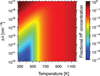
To increase the concentration of the minority charge species, increased temperatures can be used to thermally generate minority carriers and increase the H0 concentration through a shifting of the quasi-Fermi level towards mid-gap, therefore changing the occupation of electrons and holes at the energy levels of interstitial hydrogen. However, the temperature required for a given H0 concentration depends on the bulk doping density (Na) and requires higher temperatures as Na increases, as well as depending on the excess carrier concentration. For example, assuming Sah–Shockley statistics,[63,64] in 1.5-Ω cm boron-doped silicon (Na = 1 × 1016 cm−3) with a minority carrier concentration below 1 × 1014 cm−3, a temperature of at least 700 K is required to have at least 1 % of hydrogen as H0. Boron-doped silicon with Na = 1 × 1019 cm−3 requires a temperature in excess of 980 K. The use of higher temperatures also increases the diffusivity of each hydrogen charge state.[58] However, for certain defects, the temperatures required to allow sufficient diffusivity are too high to allow an effective passivation of defects owing to the thermal dissociation of hydrogen–defect and defect complexes. As a result, lower temperatures must be used to reduce the reaction rates of the dissociation reactions. Unfortunately, the temperatures required to reduce thermal dissociation sufficiently may be too low to thermally generate sufficient hydrogen in high-mobility charge states to move the hydrogen within a capture cross-section of the defects and allow passivation.
The key to increasing the mobility and reactivity of hydrogen within silicon is to change the availability of electrons and holes through minority carrier injection. Doing so modulates the fractional hydrogen charge state concentrations, and can enable effective defect passivation at low temperatures.[65] Fig. 2 shows the fractional H0 concentration as a function of temperature and excess carrier concentration (Δn) for boron-doped silicon with an acceptor doping concentration of Na = 1 × 1016 cm−3. Particularly at temperatures below 600 K, the fractional H0 concentration can be enhanced by orders of magnitude by using minority carrier injection.
|
One method to perform advanced hydrogenation processes (AHP) that generate excess carriers in the device is using illumination sources such as halogen lamps, light-emitting diodes or lasers. In this work, we opt for the use of lasers owing to their high-illumination intensity capabilities.
Hydrogenation of Structural Defects
Structural defects are often incorporated into the crystal structure of cheap, low-quality silicon common to the photovoltaic industry such as multicrystalline silicon. These structural defects include grain boundaries and dislocation clusters within the grains. In some sense, structural defects can be considered simple to passivate with hydrogen, as they are always available for passivation throughout the solar cell fabrication sequence. Nonetheless, significant evidence related to the difficulty of passivating structural defects can be found in the literature. For example, structural defects with deep energy levels have been reported to be more difficult to passivate than intra-grain defects in multicrystalline silicon.[66] The effectiveness of hydrogen passivation in multicrystalline silicon can also vary throughout the ingot, presumably owing to interactions with defects and subsequent variations in hydrogen diffusivity.[67]
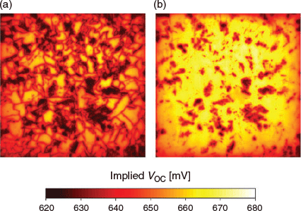
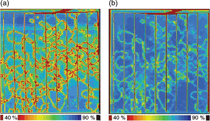
Small-angle grain boundaries, dislocations decorated with metallic impurities, and regions with high dislocation densities have proved to be more challenging to passivate using hydrogen.[68,69] An example highlighting the difficulty in passivating structural defects during conventional hydrogen passivation processes is shown in Fig. 3. Calibrated implied open circuit voltage (iVOC) maps[70] obtained from photoluminescence (PL) images[71] are shown after acidic texturing, phosphorus emitter diffusion, and the deposition of PECVD SiNx:H, and after the subsequent firing process as applied to screen-printed solar cells. The images highlight the widespread improvement in effective minority carrier lifetime of the material from the firing process, and hence, iVOC. In this instance, most grain boundaries are easily passivated during the firing process. The recombination activity of some grain boundaries and heavily dislocated regions remains, suggesting the inability of conventional hydrogenation processes for silicon solar cells to eliminate the recombination activity of such defects.
|
Further evidence is obtained on finished standard screen-printed solar cells, with significant recombination activity observed in the vicinity of the structural defects (see Fig. 4a). The reduced IQE at a wavelength of 981 nm from light-beam induced current (LBIC) measurements highlights the reduced collection of minority carriers throughout the bulk of the silicon in the vicinity of the dislocation clusters. However, the application of additional low-temperature hydrogenation processes can lead to substantial efficiency improvements in the range of 1–2 % absolute.[72–74] Fig. 4b shows the improvement in IQE in the heavily dislocated regions after an additional laser hydrogenation process (see ref. [73] for further details). These results highlight the weakness of current industrial implementations of hydrogen passivation and the importance of additional low-temperature hydrogenation processes for improving the passivation of structural defects.
|
Hydrogenation of Process-Induced Defects
Process-induced defects add an extra level of complexity for hydrogen passivation in silicon solar cells, as the defects have not necessarily been introduced by the process step where hydrogen passivation is performed. As a result, the process sequence may need to be modified to enable effective passivation of such defects.
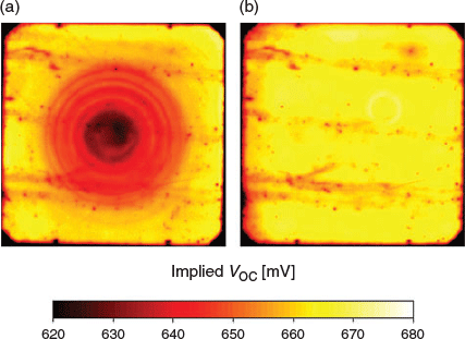
Although hydrogen passivation of process-induced defects is incredibly important and can increase the efficiency of silicon solar cells by more than 0.8 % absolute,[75] the involvement of hydrogen may often be overlooked. In many instances, hydrogen passivation naturally occurs after the introduction of the defects. For example, oxygen precipitates typically form during high-temperature processes such as emitter diffusion and oxidation.[29,76,77] Given that such processes are performed before SiNx:H deposition, particularly when such cell technologies use a subsequent firing process, hydrogen passivation may reduce the impact of those defects. For example, previous publications on screen-printed solar cells have shown a reduction in the recombination activity of oxygen precipitates after firing compared with that directly after emitter diffusion.[78,79] Although not explicitly discussed in those papers, the reduction in recombination activity is likely due to hydrogenation.[30] Although the industrial implementations of metallisation firing by Haunschild et al. were not effective at eliminating all recombination activity of oxygen precipitates, an advanced hydrogenation firing process with modified power distribution to the lamps and also incorporating minority carrier injection during the cool-down was shown to eliminate the recombination activity of oxygen precipitates completely.[30] However, further work is required to investigate the specific impact of illumination on these defects. Fig. 5a shows a calibrated iVOC map of a sample with recombination-active oxygen precipitates directly after the deposition of PECVD SiNx:H, with the corresponding map after the subsequent high-temperature advanced hydrogenation process shown in Fig. 5b, where the recombination activity has been eliminated (see refs [30] and [80] for further details).
|
Another process that can introduce defects is laser doping. A key benefit of the laser doping process is the application of localised heating, which enables localised doped regions to be formed. Another benefit is that the doping process can take place in the molten state of silicon, increasing the diffusivity of key dopants like boron and phosphorus by 6–8 orders of magnitude compared with that in the solid state using typical processing temperatures in the range of 800–1000°C.[59] This enables effective doping on the silicon within microseconds rather than the hours required for conventional approaches. However, the thermal stresses generated during the laser doping process can induce the formation of defects. For such defects, the natural passivation of the defects during solar cell fabrication depends on the process order. For example, performing laser doping before dielectric deposition has been shown to reduce or avoid defect formation.[81–84] However, performing laser doping before dielectric deposition as used by Köhler et al. in conjunction with aligned screen-printed contacts[85] also allows hydrogen passivation of the defects to occur during the SiNx:H deposition process. Further passivation of the defects may be achieved during the subsequent screen-print firing process for metal contact formation that releases hydrogen from the SiNx:H layer. Similar effects can be achieved for self-aligned plated contacts when n-type laser doping is performed before the Al–Si alloyed BSF formation.[7,86] In this instance, and for other PERC solar cells, defects generated during the laser-ablation process for rear contact formation can be consumed by the molten region or passivated by hydrogen during the Al/Si alloying process. In contrast, performing laser doping after screen-print firing means that the defects are introduced after the conventional hydrogenation process, and hence the defects will be recombination-active. Fig. 6 displays Auger-corrected inverse lifetime curves for fired wafers that have undergone laser doping followed by additional hydrogenation treatments. In this example, laser-induced defects are introduced after a typical hydrogenation process (fast-firing), resulting in a substantial increase in the Auger-corrected inverse effective minority carrier lifetime (1/τeff – 1/τAug) for all injection levels for both n-type and p-type laser doping. This reduction in τeff causes a reduction in the iVOC for both n-type and p-type laser-doped samples, from 692 and 686 mV to 661 and 670 mV respectively (see Table 1). Crystallographic defects induced by laser doping likely cause the reduction in iVOC, indicated by the introduction of a strong Shockley–Read–Hall lifetime component[87,88] and hence reduced bulk lifetime (τbulk) from values of 522 and 603 μs to 104 and 176 μs for n-type and p-type laser-doped regions respectively. No increase in dark saturation current density (J0) was observed for either n-type or p-type laser doping, indicating effective shielding of minority carriers from the exposed silicon surface. The larger drop in iVOC for the samples with n-type laser doping, particularly to a lower iVOC value than that of samples with p-type laser doping, is indicative of an increased level of recombination activity introduced by the n-type laser doping. This may be due to the laser doping occurring in the vicinity of the p-n junction, in contrast to p-type laser doping on the other surface of the test structure, ~180 μm from the p-n junction.
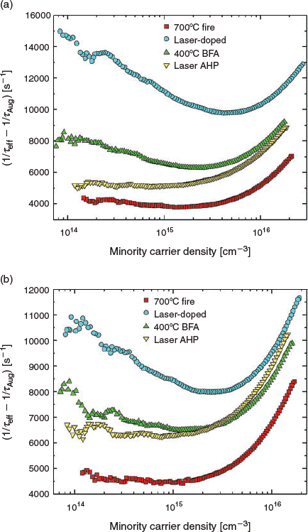
|

|
After a 400°C belt furnace anneal (BFA), a reduction in the inverse effective minority carrier lifetime was observed for all injection levels, indicating the passivation of defects induced by the laser doping process, resulting in an improvement in the 1-sun iVOC for both n-type and p-type laser-doped samples. However, the recovery in iVOC was most pronounced for the n-type case, where the iVOC increased by 16 mV, likely owing to the larger extent of recombination introduced by the n-type laser doping process. This improvement was due to the passivation of bulk defects resulting in increased τbulk values of 233 and 265 μs for n-type and p-type laser-doped regions respectively. It should be noted that for the n-type laser-doped sample, a slight increase in the J0 was observed, potentially due to an undesirable passivation of dopants in the laser-doped region. A passivation of dopants would reduce the effectiveness of the laser-doped region in shielding minority carriers from the exposed silicon surface.
The laser-based AHP led to further decrease in 1/τeff at low-injection levels for both samples, corresponding to an improved passivation of bulk defects. This improved passivation led to improvements in the τbulk to values of 360 and 335 μs for n-type and p-type laser-doped regions respectively. For the n-type laser-doped sample, this increased the iVOC value to 682 mV, with the sample showing no further change in J0. However, for the p-type laser-doped sample, an increase in inverse effective minority carrier lifetime was observed at high injections, consistent with an increase in J0. The increase in J0 counteracted the improvement in the bulk lifetime, resulting in a negligible change in iVOC. This change in J0 may be attributed to the increased mobility and reactivity of hydrogen using the AHP, enabling the passivation of dopant atoms in the p-type laser-doped region. Further work is required to avoid the increase in J0 during the passivation of laser-induced defects.
The relevant material parameters of τbulk and J0, extracted by fitting the lifetime curves, are displayed in Table 1.
If using a laser-doped selective emitter with a self-aligned metallisation scheme based on light-induced plating,[89] one option is to passivate the laser-induced defects during nickel sintering.[75] However, in this instance, a re-optimisation of the conditions may be required. For example, if the nickel sintering temperature is too low, an ineffective passivation of the laser-induced defects may result, with the solar cells subsequently requiring an additional hydrogenation process.[75] In contrast, using a higher nickel sintering temperature could adequately passivate the defects without the need for a separate hydrogenation process.[90] However, thermal constraints related to the metal contacts must be considered to avoid any unintentional alloying of Al/Si above the eutectic temperature, changes to the composition of nickel silicide for plated contacts or thermal stresses induced if the annealing or sintering is performed on the fully plated stack. As a result, particularly for process-induced defects introduced by laser processing, the process sequence may need to be modified, or the processes re-optimised to ensure effective passivation of the defects.
Hydrogenation of Carrier-Induced Defects
A variety of carrier-induced defects can be present in silicon solar cells, caused by impurities such as copper or iron.[91–93] In boron-doped Czochralski silicon, the most prominent carrier-induced degradation mechanism is caused by the simultaneous presence of boron and oxygen in the silicon material, which leads to the formation of B-O complexes.[94,95] Carrier-induced defects such as the B-O defect present a more complex problem for hydrogen passivation, in that during conventional solar cell fabrication sequences, the defects have not sufficiently formed, and therefore, cannot be passivated. It is only with prolonged exposure to carrier injection during additional processing that the defects form, and can subsequently be passivated.
A solution for mitigating B-O related carrier-induced degradation based on illuminated annealing was first proposed in 2006.[31] However, at the time, the mechanism was poorly understood. In 2009, Münzer identified a critical role of hydrogen during illuminated annealing, whereby the permanent deactivation only occurred in solar cells fabricated using hydrogen-rich SiNx:H grown by PECVD, and not those using hydrogen-lean SiNx:H grown by low-pressure chemical vapour deposition (LPCVD).[32] Further work by multiple authors has highlighted the influence of the hydrogen concentration and thickness of dielectric layers in the passivation,[16,96,97] the dependence of the passivation rate on the illumination intensity (separately from the role for defect formation[95,98]), and the correlation between the passivation rate and the theoretical concentration of H0.[31,33,60,99,100] The importance of illuminated annealing has also been noted for a more recently identified degradation mechanism.[101–103]
Despite the evidence presented for B-O defects, controversy has surrounded hydrogen’s involvement in the permanent deactivation mechanism. For example, one study presented a theory for permanent deactivation based on a purely thermal mechanism involving boron nanoprecipitates.[104] However, subsequent work demonstrated that with identical thermal profiles during fast firing, permanent recovery was only observed when samples were fired in the presence of PECVD SiNx:H,[105,106] and hence it is not completely thermal. Furthermore, a dual role of the firing process has been recently identified with the thermal elimination of defect precursors, as well as modulating the hydrogen concentration in the silicon, which leads to a change in the rate of passivation.[107]
A significant challenge for industrial boron-doped Czochralski silicon solar cells has been how to incorporate an effective illuminated annealing process into the production environment, with a throughput of 3600 wafers h−1. Early work required minutes to hours for the complete elimination of B-O-related degradation.[33,108–110] To speed up reaction rates, higher temperatures could be used. However, the increased reaction rates of desirable reactions to enable defect passivation, including defect formation and defect passivation, are counteracted by the dissociation of the hydrogen–defect complex and the dissociation of the B-O defect.[111,112] Both of these reactions reduce the availability of defects for passivation, particularly at elevated temperatures owing to the higher activation energies of those reactions. Therefore, they place an upper limit on the temperature that can be used to effectively mitigate carrier-induced degradation for a specific sample and processing condition. Using typical conditions with low-intensity light, only temperatures below ~230°C could enable effective passivation of the B-O defects, with incomplete passivation occurring at higher temperatures.[110]
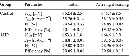
In contrast, by accelerating the defect formation rate using high-intensity illumination, a substantially higher temperature can be used, which results in a further reduction in the time to form the defects.[72,98,100] Using such a process, B-O defects can be completely formed and passivated on finished industrial screen-printed solar cells in less than 8 s,[72,100,113] which can improve cell performance of industrial cells in the vicinity of 1 % absolute.[113] This has seen the development of new halogen-, light-emitting diode (LED)-, and laser-based industrial advanced hydrogenation tools for the mitigation of B-O-related degradation.[113] An example showing the impact of advanced hydrogenation processes for eliminating B-O-related degradation is shown in Table 2. The cells that received an AHP process to eliminate B-O-related carrier-induced degradation show a higher efficiency (20.54 %) after the AHP and subsequent accelerated stability test[98] compared with the initial efficiency (20.11 %). This increase was related to significant increases in the VOC and short circuit current (JSC) of the devices, indicating the passivation of additional defects in the device. Furthermore, no significant increase in the standard deviation was observed for the electrical parameters. In contrast, cells that did not receive an AHP saw a drop in efficiency after the stability test from 20.11 to 19.42 %. This was due to a reduction in VOC, JSC, and fill factor (FF). Furthermore, a larger spread of the electrical parameters was measured on the industrial cells after stability testing. Hence, the AHP led to an improvement in the stable cell performance of 1.1 % absolute compared with the control samples.
|
Conclusions
The present paper discussed the challenges of passivating structural, process-induced, and carrier-induced defects. Although structural defects are typically easy to passivate owing to always being present in the wafer, they can still benefit from the application of hydrogen passivation processes incorporating minority carrier injection. The implementation of such processes can improve the IQE in dislocated regions of cast silicon material. For process-induced defects, careful attention must be paid to the order of processing to ensure that a hydrogen passivation process is performed after the introduction of the defects. For defects such as oxygen precipitates, the defects can naturally be passivated during subsequent high-temperature firing processes. However, for laser-induced defects, additional hydrogenation processes should be used if the defects are introduced after the typical hydrogenation process used for solar cell fabrication. Advanced hydrogenation processes show an improved level of passivation for laser-induced defects in the bulk. However, the processes can also lead to an undesirable increase in the J0 due to the passivation of dopant atoms in the laser-doped region. Further work is required to avoid this increase in J0 and the reduced effectiveness of shielding minority carriers from the exposed silicon surface.
For carrier-induced defects, typically, the defects have not formed by the end of solar cell fabrication, and a dedicated process with carrier injection must be performed to both form the defects and manipulate the hydrogen charge states to enable defect passivation. The implementation of advanced hydrogenation processes to eliminate B-O-related degradation can increase the stable performance of industrial PERC solar cells by 1.1 % absolute using new commercial laser-based advanced hydrogenation tools.
Methodology
For hydrogen charge state occupation, a model to predict charge state distributions was developed in Matlab based on the work by Sun et al. using Sah–Shockley statistics.[63,64] This present work assumes a hydrogen acceptor energy level of 0.07 eV below mid-gap and a donor energy level of 0.16 eV below the conduction band.[58] The capture cross-section ratios assumed for the acceptor and donor levels are 0.05 and 1 respectively.[63]
For laser-induced defect experiments, laser doping was performed on industrially processed 6″ (156 mm) PERC cell lifetime test structures. The p-type boron-doped Czochralski silicon grown wafers had a thickness of ~180 μm and resistivity of ~1.6 Ω cm. The structure included a phosphorus emitter on the front surface, passivated by thermal oxide and PECVD SiNx:H. On the rear surface, a stack of aluminium oxide and PECVD SiNx:H was used. Prior to laser doping, wafers were fired with a peak temperature of ~620°C in an industrial belt furnace.
For n-type laser-doped samples, phosphoric acid was spun onto the front surface as a dopant source. For p-type laser doping, the rear aluminium oxide layer was used as a dopant source.[114] Laser doping was performed on the front surface for n-type doping and the rear surface for p-type doping using a 532-nm continuous wave Newport laser with a spot size of ~20 μm. For the n-type doping, a power of 14 W and a speed of 2 m s−1 were used. P-type doping was performed with a power of 21 W and a speed of 6 m s−1.
After laser doping, phosphoric acid was removed in water (where relevant). Then, wafers received a rapid BFA at 400°C. Finally, an AHP was performed with a 938-nm laser operating in continuous wave mode at 300°C for 10 s with an illumination intensity of ~100 suns.
Lifetime measurements were obtained at various stages using a quasi-steady-state photoconductance tool (QSS-PC) (Sinton Instruments WCT-120)[115] and analysed using the generalised method.[116] Measured data were corrected for Auger recombination using the Richter model.[117] Effective minority carrier lifetimes were extracted at an excess minority carrier density (Δn) of 1 × 1015 cm−3 (equal to ~10 % of the background boron dopant density).
For the passivation of B-O defects, industrially fabricated 6″ p-type Czochralski PERC solar cells were used. Finished cells were dark-annealed at 260°C for 20 min to dissociate B-O defects.[118] Advanced hydrogenation was performed in a commercially available DR Laser tool at 240°C, with 45 kW m−2 of 980-nm illumination for 10 s. An accelerated stability test was performed in the same laser tool [98,103] on control cells and the laser-hydrogenated cells at a temperature of 135°C, with 45 kW m−2 of 980-nm illumination for 10 s.
Current density–voltage (J–V) measurements were obtained on a HALM tester with class AAA spectrum at room temperature.
Conflicts of Interest
The authors declare no conflicts of interest.
Acknowledgements
This work was supported in part by the Australian Government through the Australian Renewable Energy Agency (ARENA) and the Australian Centre for Advanced Photovoltaics and in part by the UK Institution of Engineering and Technology (IET) through the A. F. Harvey Engineering Prize. Brett Hallam would also like to acknowledge the Australian Research Council (ARC) through grant number DE170100620 and the Australian Academy of Science through the J. G. Russell Prize. Responsibility for the views, information, or advice expressed herein is not accepted by the Australian Government. The authors would like to thank the processing team in the Solar Industrial Research Facility at UNSW, and Daniel Chen and Moonyong Kim for their contributions to sample processing and characterisation.
References
[1] VDMA Photovoltaic Equipment, International Technology Roadmap for Photovoltaic: 2016 Results 2017, Frankfurt, Germany.[2] VDMA Photovoltaic Equipment, International Technology Roadmap for Photovoltaic: Germany 2018, Frankfurt, Germany.
[3] http://pvinsights.com (accessed 29 August 2018).
[4] C. Boehme, G. Lucovsky, J. Appl. Phys. 2000, 88, 6055.
| Crossref | GoogleScholarGoogle Scholar |
[5] G. Dingemans, M. C. M. van de Sanden, W. M. M. Kessels, Electrochem. Solid-State Lett. 2010, 13, H76.
| Crossref | GoogleScholarGoogle Scholar |
[6] Z. Wang, P. Han, H. Lu, H. Qian, L. Chen, Q. Meng, N. Tang, F. Gao, Y. Jia, J. Wu, W. Wu, H. Zhu, J. Ji, Z. Shi, A. Sugianto, L. Mai, B. Hallam, S. Wenham, Prog. Photovolt. Res. Appl. 2012, 20, 260.
| Crossref | GoogleScholarGoogle Scholar |
[7] M. Kim, D. Kyeong, K. Lee, W. Lee, E.-C. Cho, in 40th IEEE Photovoltaic Specialist Conference (PVSC) 2014, pp. 2823–2827 (IEEE: Piscataway, NJ).
[8] P. Saint-Cast, J. Benick, D. Kania, L. Weiss, M. Hofmann, J. Rentsch, R. Preu, S. W. Glunz, IEEE Electron Device Lett. 2010, 31, 695.
| Crossref | GoogleScholarGoogle Scholar |
[9] I. Cesar, E. Granneman, P. Vermont, H. Khatri, H. Kerp, A. Shaikh, P. Manshanden, A. A. Mewe, I. G. Romijn, A. W. Weeber, in 37th IEEE Photovoltaic Specialists Conference 2011, pp. 1405–1410 (IEEE: Piscataway, NJ).
[10] F. Chen, I. Romijn, A. Weeber, J. Tan, B. Hallam, J. Cotter, in Proceedings of the 22nd European Photovoltaic Solar Energy Conference 2007, pp. 1053–1060 (WIP: Munich).
[11] B. Hallam, B. Tjahjono, S. Wenham, Sol. Energy Mater. Sol. Cells 2012, 96, 173.
| Crossref | GoogleScholarGoogle Scholar |
[12] B. Hoex, S. B. S. Heil, E. Langereis, M. C. M. de Sanden, W. M. M. Kessels, Appl. Phys. Lett. 2006, 89, 42112.
| Crossref | GoogleScholarGoogle Scholar |
[13] J. Schmidt, M. Kerr, Sol. Energy Mater. Sol. Cells 2001, 65, 585.
| Crossref | GoogleScholarGoogle Scholar |
[14] G. Agostinelli, A. Delabie, P. Vitanov, Z. Alexieva, H. F. W. Dekkers, S. De Wolf, G. Beaucarne, Sol. Energy Mater. Sol. Cells 2006, 90, 3438.
| Crossref | GoogleScholarGoogle Scholar |
[15] S. Wilking, A. Herguth, G. Hahn, Energy Procedia 2013, 38, 642.
| Crossref | GoogleScholarGoogle Scholar |
[16] S. Dubois, F. Tanay, J. Veirman, N. Enjalbert, J. Stendera, S. Butté, P. Pochet, D. Caliste, Y. Mao, D. Timerkaeva, D. Blanc, K. Fraser, M. Lemiti, O. Palais, I. Périchaud, B. Dridi Rezgui, V. Mong-The Yen, M. Pasquinelli, M. Gerard, F. Madon, N. Le Quang, in 27th European Photovoltaic Solar Energy Conference 2012, pp. 749–754 (WIP: Munich).
[17] W. Soppe, H. Rieffe, A. Weeber, Prog. Photovolt. Res. Appl. 2005, 13, 551.
| Crossref | GoogleScholarGoogle Scholar |
[18] B. Hallam, D. Chen, M. Kim, B. Stefani, B. Hoex, M. Abbott, S. Wenham, Phys. Status Solidi. A: Appl. Mater. Sci. 2017, 214, 1700305.
| Crossref | GoogleScholarGoogle Scholar |
[19] A. G. Aberle, Sol. Energy Mater. Sol. Cells 2001, 65, 239.
| Crossref | GoogleScholarGoogle Scholar |
[20] R. Lüdemann, Mater. Sci. Eng. B 1999, 58, 86.
| Crossref | GoogleScholarGoogle Scholar |
[21] Z. Chen, A. Rohatgi, R. O. Bell, J. P. Kalejs, Appl. Phys. Lett. 1994, 65, 2078.
| Crossref | GoogleScholarGoogle Scholar |
[22] F. Duerinckx, J. Szlufcik, Sol. Energy Mater. Sol. Cells 2002, 72, 231.
| Crossref | GoogleScholarGoogle Scholar |
[23] R. Einhaus, F. Duerinckx, E. Van Kerschaver, J. Szlufcik, F. Durand, P. J. Ribeyron, J. C. Duby, D. Sarti, G. Goaer, G. N. Le, Mater. Sci. Eng. B 1999, 58, 81.
| Crossref | GoogleScholarGoogle Scholar |
[24] L. J. Geerligs, A. Azzizi, D. H. Macdonald, P. Manshanden, in 13th Workshop on Crystalline Silicon Solar Cell Materials and Processes 2003, pp. 199–202 (National Renewable Energy Laboratory: Golden, CO).
[25] R. Singh, S. J. Fonash, A. Rohatgi, Appl. Phys. Lett. 1986, 49, 800.
| Crossref | GoogleScholarGoogle Scholar |
[26] A. J. Tavendale, S. J. Pearton, J. Phys. C: Solid State Phys. 1983, 16, 1665.
| Crossref | GoogleScholarGoogle Scholar |
[27] N. H. Nickel, N. M. Johnson, W. B. Jackson, Appl. Phys. Lett. 1993, 62, 3285.
| Crossref | GoogleScholarGoogle Scholar |
[28] N. Yarykin, J. U. Sachse, H. Lemke, J. Weber, Phys. Rev. B Condens. Matter Mater. Phys. 1999, 59, 5551.
| Crossref | GoogleScholarGoogle Scholar |
[29] R. J. Falster, D. Gambaro, M. Cornara, M. Olmo, M. Pagani, Solid State Phenom. 1997, 57–58, 123.
| Crossref | GoogleScholarGoogle Scholar |
[30] B. J. Hallam, C. E. Chan, M. D. Abbott, S. R. Wenham, Sol. Energy Mater. Sol. Cells 2015, 141, 125.
| Crossref | GoogleScholarGoogle Scholar |
[31] A. Herguth, G. Schubert, M. Käs, G. Hahn, in 4th IEEE World Conference on Photovoltaic Energy Conversion 2006, 1, pp. 940–943 (IEEE: Piscataway, NJ).
[32] K. Münzer, in 24th European Photovoltaic Solar Energy Conference 2009, pp. 1558–1561 (WIP: Munich).
[33] A. Herguth, G. Schubert, M. Käs, G. Hahn, Prog. Photovolt. Res. Appl. 2008, 16, 135.
| Crossref | GoogleScholarGoogle Scholar |
[34] P. Balk, in Electrochemical Society Spring Meeting 1965, 14, pp. 237–240 (The Electrochemical Society: Pennington, NJ).
[35] B. E. Deal, E. L. MacKenna, P. L. Castro, J. Electrochem. Soc. 1969, 116, 997.
| Crossref | GoogleScholarGoogle Scholar |
[36] A. W. Blakers, A. Wang, A. M. Milne, J. Zhao, M. A. Green, Appl. Phys. Lett. 1989, 55, 1363.
| Crossref | GoogleScholarGoogle Scholar |
[37] R. R. King, R. A. Sinton, R. M. Swanson, IEEE Trans. Electron Dev. 1990, 37, 365.
| Crossref | GoogleScholarGoogle Scholar |
[38] R. M. Swanson, U.S. Patent 4927770 1990.
[39] J. Zhao, A. Wang, P. P. Altermatt, S. R. Wenham, M. A. Green, Sol. Energy Mater. Sol. Cells 1996, 41–42, 87.
| Crossref | GoogleScholarGoogle Scholar |
[40] J. Zhao, A. Wang, M. A. Green, Sol. Energy Mater. Sol. Cells 2001, 66, 27.
| Crossref | GoogleScholarGoogle Scholar |
[41] K. Yoshikawa, H. Kawasaki, W. Yoshida, T. Irie, K. Konishi, K. Nakano, T. Uto, D. Adachi, M. Kanematsu, H. Uzu, K. Yamamoto, Nat. Energy 2017, 2, 17032.
[42] M. Taguchi, A. Yano, S. Tohoda, K. Matsuyama, Y. Nakamura, T. Nishiwaki, K. Fujita, E. Maruyama, IEEE J. Photovoltaics 2014, 4, 96.
| Crossref | GoogleScholarGoogle Scholar |
[43] S. W. Glunz, F. Feldmann, A. Richter, M. Bivour, C. Reichel, H. Steinkemper, J. Benick, M. Hermle, in Proceedings of the 31st European Photovoltaic Solar Energy Conference and Exhibition 2015, pp. 259–263 (WIP: Munich).
[44] A. Richter, J. Benick, F. Feldmann, A. Fell, M. Hermle, S. W. Glunz, Sol. Energy Mater. Sol. Cells 2017, 173, 96.
| Crossref | GoogleScholarGoogle Scholar |
[45] P. J. Cousins, D. D. Smith, H.-C. Luan, J. Manning, T. D. Dennis, A. Waldhauer, K. E. Wilson, G. Harley, W. P. Mulligan, in 35th IEEE Photovoltaic Specialists Conference 2010, pp. 275–278 (IEEE: Piscataway, NJ).
[46] W. P. Mulligan, M. J. Cudzinovic, T. Pass, D. Smith, R. M. Swanson, U.S. Patent 7388147 2008.
[47] M. Taguchi, M. Tanaka, T. Matsuyama, T. Matsuoka, S. Tsuda, S. Nakano, Y. Kishi, Y. Kuwano, in Proceedings of the Fifth International Photovoltaic Science and Engineering Conference 1990, pp. 689–692 (Publ. Office Internat. PVSEC-5: Kyoto).
[48] S. De Wolf, A. Descoeudres, Z. C. Holman, C. Ballif, Green 2012, 2, 7.
| Crossref | GoogleScholarGoogle Scholar |
[49] J. B. Heng, C. Yu, Z. Xu, J. Fu, U.S. Patent 8686283 2014.
[50] A. B. Turner, O. Schultz-Wuttnann, D. De Ceuster, D. E. Crafts, U.S. Patent 20120186649 2010.
[51] J. Zhao, A. Wang, in Proceedings of the 4th IEEE World Conference on Photovoltaic Energy Conversion 2006, 1, pp. 996–999 (IEEE: Piscataway, NJ).
[52] P. Saint-Cast, D. Kania, M. Hofmann, J. Benick, J. Rentsch, R. Preu, Appl. Phys. Lett. 2009, 95, 151502.
| Crossref | GoogleScholarGoogle Scholar |
[53] A. Urueña, M. Aleman, E. Cornagliotti, A. Sharma, M. Haslinger, L. Tous, R. Russell, J. John, F. Duerinckx, J. Szlufcik, Prog. Photovolt. Res. Appl. 2016, 24, 1149.
| Crossref | GoogleScholarGoogle Scholar |
[54] X. Yang, J. Bullock, Q. Bi, K. Weber, Appl. Phys. Lett. 2015, 106, 113901.
[55] J. Zhu, N. M. Johnson, C. Herring, Phys. Rev. B 1990, 41, 12354.
| Crossref | GoogleScholarGoogle Scholar |
[56] D. Mathiot, Phys. Rev. B 1989, 40, 5867.
| Crossref | GoogleScholarGoogle Scholar |
[57] C. H. Seager, R. A. Anderson, Appl. Phys. Lett. 1988, 53, 1181.
| Crossref | GoogleScholarGoogle Scholar |
[58] C. Herring, N. M. Johnson, C. G. de Walle, Phys. Rev. B 2001, 64, 125209.
| Crossref | GoogleScholarGoogle Scholar |
[59] K. Tang, E.J. Øvrelid, G. Tranell, M. Tangstad, in Crystal Growth of Si for Solar Cells (Eds K. Nakajima, N. Usami) 2009, pp. 219–251 (Springer: New York, NY).
[60] M. Gläser, D. Lausch, Energy Procedia 2015, 77, 592.
| Crossref | GoogleScholarGoogle Scholar |
[61] C. H. Seager, R. A. Anderson, Appl. Phys. Lett. 1991, 59, 585.
| Crossref | GoogleScholarGoogle Scholar |
[62] C. T. Sah, J. Y. C. Sun, J. J. T. Tzou, Appl. Phys. Lett. 1983, 43, 204.
| Crossref | GoogleScholarGoogle Scholar |
[63] C. Sun, F. E. Rougieux, D. Macdonald, J. Appl. Phys. 2015, 117, 45702.
| Crossref | GoogleScholarGoogle Scholar |
[64] C.-T. Sah, R. N. Noyce, W. Shockley, Proc. IRE 1957, 45, 1228.
| Crossref | GoogleScholarGoogle Scholar |
[65] S. R. Wenham, P. G. Hamer, B. J. Hallam, A. Sugianto, C. E. Chan, L. Song, P. H. Lu, A. M. Wenham, L. Mai, C. M. Chong, G. X. Xu, M. B. Edwards, U.S. Patent 9190556 2015.
[66] S. Martinuzzi, I. Périchaud, F. Warchol, Sol. Energy Mater. Sol. Cells 2003, 80, 343.
| Crossref | GoogleScholarGoogle Scholar |
[67] M. Sheoran, A. Upadhyaya, A. Rohatgi, Solid-State Electron. 2008, 52, 612.
| Crossref | GoogleScholarGoogle Scholar |
[68] J. Chen, D. Yang, Z. Xi, T. Sekiguchi, Physica B 2005, 364, 162.
| Crossref | GoogleScholarGoogle Scholar |
[69] M. Sheoran, Development of High-Efficiency Solar Cells on Thin Silicon through Design Optimization and Defect Passivation 2009, Ph.D. thesis, Georgia Institute of Technology, Georgia.
[70] B. Hallam, B. Tjahjono, T. Trupke, S. Wenham, J. Appl. Phys. 2014, 115, 44901.
| Crossref | GoogleScholarGoogle Scholar |
[71] T. Trupke, R. A. Bardos, M. C. Schubert, W. Warta, Appl. Phys. Lett. 2006, 89, 44107.
| Crossref | GoogleScholarGoogle Scholar |
[72] B. J. B. J. Hallam, P. G. P. G. Hamer, S. Wang, L. Song, N. Nampalli, M. D. M. D. Abbott, C. E. C. E. Chan, D. Lu, A. M. A. M. Wenham, L. L. Mai, N. Borojevic, A. Li, D. Chen, M. Y. Y. Kim, A. Azmi, S. Wenham, Energy Procedia 2015, 77, 799.
| Crossref | GoogleScholarGoogle Scholar |
[73] A. Wenham, L. Song, M. Abbott, I. Zafirovska, S. Wang, B. Hallam, C. Chan, A. Barnett, S. Wenham, Front. Energy 2017, 11, 60.
| Crossref | GoogleScholarGoogle Scholar |
[74] L. Song, A. Wenham, S. Wang, P. Hamer, M. S. Ahmmed, B. Hallam, L. Mai, M. Abbott, E. R. Hawkes, C. Chong, S. Wenham, Int. J. Photoenergy 2015, 2015, 1.
| Crossref | GoogleScholarGoogle Scholar |
[75] B. Hallam, A. Sugianto, L. Mai, G. Xu, C. Chan, M. Abbott, S. Wenham, A. Uruena, E. Cornagliotti, M. Aleman, IEEE J. Photovoltaics 2014, 4, 1413.
| Crossref | GoogleScholarGoogle Scholar |
[76] P. E. Freeland, K. A. Jackson, C. W. Lowe, J. R. Patel, Appl. Phys. Lett. 1977, 30, 31.
| Crossref | GoogleScholarGoogle Scholar |
[77] V. V. Voronkov, R. Falster, J. Cryst. Growth 1999, 204, 462.
| Crossref | GoogleScholarGoogle Scholar |
[78] J. Haunschild, I. E. Reis, J. Geilker, S. Rein, Phys. Status Solidi Rapid Res. Lett. 2011, 5, 199.
| Crossref | GoogleScholarGoogle Scholar |
[79] J. Haunschild, M. Glatthaar, M. Demant, J. Nievendick, M. Motzko, S. Rein, E. R. Weber, Sol. Energy Mater. Sol. Cells 2010, 94, 2007.
| Crossref | GoogleScholarGoogle Scholar |
[80] B. J. J. Hallam, P. G. G. Hamer, S. R. R. Wenham, M. D. D. Abbott, A. Sugianto, A. M. M. Wenham, C. E. E. Chan, G. Xu, J. Kraiem, J. Degoulange, R. Einhaus, IEEE J. Photovoltaics 2014, 4, 88.
| Crossref | GoogleScholarGoogle Scholar |
[81] A. Sugianto, B. S. Tjahjono, J. H. Guo, S. R. Wenham, in Proceedings of the 22nd European Photovoltaic Solar Energy Conference 2007, pp. 1759–1762 (WIP: Munich).
[82] D. Kray, A. Fell, S. Hopman, K. Mayer, G. P. Willeke, S. W. Glunz, Appl. Phys., A Mater. Sci. Process. 2008, 93, 99.
| Crossref | GoogleScholarGoogle Scholar |
[83] U. Jaeger, M. Okanovic, M. Hörteis, A. Grohe, R. Preu, in Proceedings of the 24th European Photovoltaic Solar Energy Conference 2009, pp. 1740–1743 (WIP: Munich).
[84] Z. Hameiri, T. Puzzer, L. Mai, A. B. Sproul, S. R. Wenham, Prog. Photovolt. Res. Appl. 2011, 19, 391.
| Crossref | GoogleScholarGoogle Scholar |
[85] J. R. Köhler, P. Grabitz, S. Eisele, T. Röder, J. H. Werner, Proceedings of the 24th European Photovoltaic Solar Energy Conference 2009, pp. 1847–1850 (WIP: Munich).
[86] B. Hallam, A. Urueña, R. Russell, M. Aleman, M. Abbott, C. Dang, S. Wenham, L. Tous, J. Poortmans, Sol. Energy Mater. Sol. Cells 2015, 89.
[87] W. Shockley, W. T. Read, Phys. Rev. 1952, 87, 835.
| Crossref | GoogleScholarGoogle Scholar |
[88] R. N. Hall, Phys. Rev. 1952, 87, 387.
| Crossref | GoogleScholarGoogle Scholar |
[89] B. Hallam, S. Wenham, A. Sugianto, L. Mai, C. Chong, M. Edwards, D. Jordan, P. Fath, IEEE J. Photovoltaics 2011, 1, 43.
| Crossref | GoogleScholarGoogle Scholar |
[90] B. Hallam, High-Efficiency Laser-Doped Silicon Solar Cells with Advanced Hydrogenation 2014, Ph.D. thesis, University of New South Wales, Sydney, Australia.
[91] S. D. Brotherton, P. Bradley, A. Gill, J. Appl. Phys. 1985, 57, 1941.
| Crossref | GoogleScholarGoogle Scholar |
[92] D. H. Macdonald, L. J. Geerligs, A. Azzizi, J. Appl. Phys. 2004, 95, 1021.
| Crossref | GoogleScholarGoogle Scholar |
[93] A. Inglese, J. Lindroos, H. Savin, Appl. Phys. Lett. 2015, 107, 52101.
| Crossref | GoogleScholarGoogle Scholar |
[94] J. Knobloch, S. W. Glunz, V. Henninger, W. Warta, W. Wettling, F. Schomann, W. Schmidt, A. Endros, K. Münzer, A. Endrös, K. A. Münzer, in Proceedings of the 13th European Photovoltaic Solar Energy Conference 1995, pp. 9–12 (WIP: Munich).
[95] J. Schmidt, K. Bothe, Phys. Rev. B Condens. Matter Mater. Phys. 2004, 69, 24107.
| Crossref | GoogleScholarGoogle Scholar |
[96] G. Krugel, W. Wolke, J. Geilker, S. Rein, R. Preu, Energy Procedia 2011, 8, 47.
| Crossref | GoogleScholarGoogle Scholar |
[97] S. Wilking, A. Herguth, G. Hahn, J. Appl. Phys. 2013, 113, 194503.
| Crossref | GoogleScholarGoogle Scholar |
[98] P. Hamer, B. Hallam, M. Abbott, S. Wenham, Phys. Status Solidi Rapid Res. Lett. 2015, 9, 297.
| Crossref | GoogleScholarGoogle Scholar |
[99] B. Lim, S. Hermann, K. Bothe, J. Schmidt, R. Brendel, in 23rd European Photovoltaic Solar Energy Conference 2008, pp. 1018–1022 (WIP: Munich).
[100] P. Hamer, B. Hallam, M. Abbott, C. Chan, N. Nampalli, S. Wenham, Sol. Energy Mater. Sol. Cells 2016, 145, 440.
| Crossref | GoogleScholarGoogle Scholar |
[101] K. Ramspeck, S. Zimmermann, H. Nagel, A. Metz, Y. Gassenbauer, B. Birkmann, A. Seidl, in Proceedings of the 27th European Photovoltaic Solar Energy Conference 2012, 1, pp. 861–865 (WIP: Munich).
[102] F. Kersten, P. Engelhart, H.-C. Ploigt, A. Stekolnikov, T. Lindner, F. Stenzel, M. Bartzsch, A. Szpeth, K. Petter, J. Heitmann, J. Müller, in 42nd IEEE Photovoltaic Specialist Conference 2015, pp. 1–5 (IEEE: Piscataway, NJ).
[103] D. N. R. Payne, C. E. Chan, B. J. Hallam, B. Hoex, M. D. Abbott, S. R. Wenham, D. M. Bagnall, Phys. Status Solidi Rapid Res. Lett. 2016, 10, 237.
| Crossref | GoogleScholarGoogle Scholar |
[104] D. C. Walter, B. Lim, K. Bothe, V. V. Voronkov, R. Falster, J. Schmidt, Appl. Phys. Lett. 2014, 104, 42111.
| Crossref | GoogleScholarGoogle Scholar |
[105] N. Nampalli, B. Hallam, C. Chan, M. Abbott, S. Wenham, Appl. Phys. Lett. 2015, 106, 173501.
| Crossref | GoogleScholarGoogle Scholar |
[106] N. Nampalli, B. J. J. Hallam, C. E. E. Chan, M. D. D. Abbott, S. R. R. Wenham, IEEE J. Photovoltaics 2015, 5, 1580.
| Crossref | GoogleScholarGoogle Scholar |
[107] N. Nampalli, H. Li, M. Kim, B. Stefani, S. Wenham, B. Hallam, M. Abbott, Sol. Energy Mater. Sol. Cells 2017, 173.
[108] A. Herguth, G. Schubert, M. Kaes, G. Hahn, in IEEE 4th World Conference on Photovoltaic Energy Conversion 2006, pp. 940–943 (IEEE: Piscataway, NJ).
[109] B. Lim, K. Bothe, J. Schmidt, Phys. Status Solidi Rapid Res. Lett. 2008, 2, 93.
| Crossref | GoogleScholarGoogle Scholar |
[110] S. Wilking, C. Beckh, S. Ebert, A. Herguth, G. Hahn, Sol. Energy Mater. Sol. Cells 2014, 131, 2.
| Crossref | GoogleScholarGoogle Scholar |
[111] B. J. J. Hallam, M. D. Abbott, N. Nampalli, P. G. G. Hamer, S. R. R. Wenham, IEEE J. Photovoltaics 2016, 6, 92.
| Crossref | GoogleScholarGoogle Scholar |
[112] B. Hallam, M. Abbott, N. Nampalli, P. Hamer, S. Wenham, J. Appl. Phys. 2016, 119, 65701.
| Crossref | GoogleScholarGoogle Scholar |
[113] B. J. Hallam, C. E. Chan, R. Chen, S. Wang, J. Ji, L. Mai, M. D. Abbott, D. N. R. Payne, M. Kim, D. Chen, C. Chong, S. R. Wenham, Jpn. J. Appl. Phys. 2017, 56, 08MB13.
| Crossref | GoogleScholarGoogle Scholar |
[114] E. Cornagliotti, A. Uruena, B. Hallam, L. Tous, R. Russell, F. Duerinckx, J. Szlufcik, Sol. Energy Mater. Sol. Cells 2015, 138.
[115] R. A. Sinton, A. Cuevas, M. Stuckings, in Proceedings of the 25th IEEE Photovoltaic Specialists Conference 1996, pp. 457–460 (IEEE: Piscataway, NJ).
[116] H. Nagel, C. Berge, A. G. Aberle, J. Appl. Phys. 1999, 86, 6218.
| Crossref | GoogleScholarGoogle Scholar |
[117] A. Richter, S. W. Glunz, F. Werner, J. Schmidt, A. Cuevas, Phys. Rev. B 2012, 86, 165202.
| Crossref | GoogleScholarGoogle Scholar |
[118] K. Bothe, J. Schmidt, J. Appl. Phys. 2006, 99, 13701.
| Crossref | GoogleScholarGoogle Scholar |
* Brett J. Hallam is the recipient of the 2017 J. G. Russell Prize from the Australian Academy of Science.